Why Glass Substrates Are the Next Massive Leap in Semiconductor Packaging
As AI chips grow larger and hotter, traditional plastic-like substrates are warping under the strain. The semiconductor industry is now racing to replace them with glass, unlocking unprecedented density, thermal stability, and speed.
By Factlen Editorial Team
- Chip Manufacturers
- View glass substrates as an existential necessity to sustain Moore's Law and capture the high-margin AI data center market.
- Packaging Engineers
- Focus on the physical realities of manufacturing, specifically mitigating glass brittleness and interface stress on the factory floor.
- AI Architects
- Eager for the massive bandwidth, thermal stability, and density gains that glass unlocks for next-generation multi-chiplet processors.
What's not represented
- · Consumer Electronics Manufacturers
- · Environmental Regulators
Why this matters
The physical limits of current chip packaging are bottlenecking the advancement of artificial intelligence and high-performance computing. Transitioning to glass substrates allows the tech industry to sustain Moore's Law, paving the way for vastly more powerful, energy-efficient data centers and eventually consumer electronics.
Key points
- Traditional organic chip substrates warp under the extreme heat of modern AI processors.
- Glass substrates offer ultra-low thermal expansion that perfectly matches silicon, preventing warping.
- The extreme flatness of glass allows for a 10x increase in interconnect density.
- Intel showcased a crack-free glass core sample in early 2026, targeting mass production by 2030.
- Manufacturing challenges remain, particularly regarding the brittleness and optical inspection of glass.
The artificial intelligence boom is hitting a physical bottleneck, but the problem isn't the silicon itself—it is the foundation the silicon sits on. As tech giants race to build increasingly massive AI processors, the underlying materials that connect these chips to the rest of the computer are reaching their absolute physical limits.[1]
This foundation is known as the substrate. It acts as the critical translator between the microscopic, nanometer-scale connections of a silicon chip and the macroscopic, millimeter-scale connections of a printed circuit board. Without a highly engineered substrate, a modern processor simply cannot communicate with a computer's memory or power supply.[1]
For decades, the semiconductor industry has relied on organic substrates—complex layers of plastic-like resins and fiberglass. However, as modern chips grow larger and consume hundreds of watts of power, these organic materials are beginning to fail. Under extreme heat, organic substrates are prone to warping, which can snap delicate connections and destroy the processor.[2]
The root of this warping lies in thermal expansion. When a silicon chip heats up under heavy computational loads, it expands at a specific rate. Organic plastics expand at a vastly different, much faster rate. This mismatch in the "coefficient of thermal expansion" (CTE) creates immense mechanical stress, bending the package out of shape.[6]

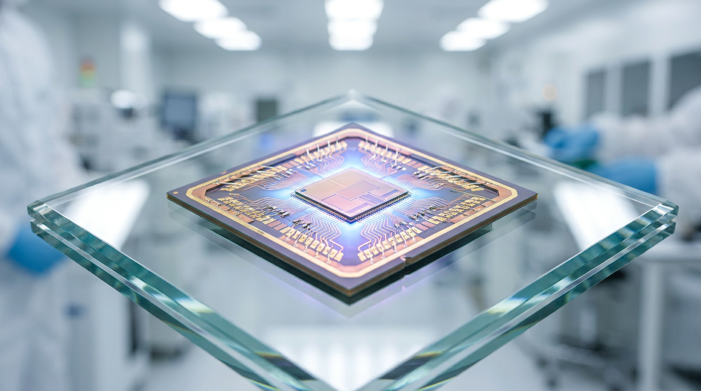
To solve this, the industry is turning to a material that has been used in optics and displays for centuries: glass. By replacing the organic core of the substrate with highly engineered glass, semiconductor manufacturers have found a material that remains perfectly flat and rigid even under extreme thermal loads.[2]
Glass possesses an ultra-low coefficient of thermal expansion that can be tuned to closely mirror that of silicon. When an AI processor heats up, the glass substrate expands at the exact same rate as the chip above it. This harmonious expansion eliminates the warping that plagues modern high-performance processors, ensuring long-term reliability.[6]
Beyond thermal stability, glass offers a massive leap in connection density. Because glass is exceptionally flat and dimensionally stable, manufacturers can etch significantly finer circuit patterns onto its surface. Intel estimates that glass substrates enable a tenfold increase in interconnect density compared to today's organic limits, alongside a 50% reduction in pattern distortion.[2]
The benefits extend to electrical performance as well. Glass features a lower dielectric constant than organic resins, which minimizes signal propagation delays and crosstalk between adjacent wires. This allows data to move faster and more efficiently, a critical requirement for high-frequency 5G communications and data-hungry AI workloads.[3]
Glass features a lower dielectric constant than organic resins, which minimizes signal propagation delays and crosstalk between adjacent wires.
To move power and data vertically through the package, engineers utilize Through-Glass Vias (TGVs). These are microscopic holes drilled directly through the glass core using advanced lasers, which are then filled with conductive copper. TGVs allow for tighter integration of components and drastically shorter signal paths, reducing overall power consumption.[6]

The urgent push for glass is driven almost entirely by the architectural demands of artificial intelligence. Modern AI processors are no longer single, monolithic pieces of silicon. Instead, they rely on "chiplets"—multiple smaller, specialized chips stitched together into a massive, unified complex.[1]
Organic substrates are struggling to support the sheer physical size of these new chiplet complexes. Glass provides the mechanical rigidity needed to assemble ultra-large form-factor packages without sacrificing manufacturing yield. It also allows architects to embed optical interconnects, inductors, and capacitors directly into the glass at higher temperatures.[2]
The commercial race to perfect this technology is accelerating rapidly. In early 2026, Intel showcased a major milestone at the NEPCON Japan exhibition, debuting its first functional sample combining its proprietary EMIB packaging technology with a glass core substrate.[4]
Intel's prototype measured roughly 1,700 square millimeters and featured a complex 22-layer stack with an 800-micrometer thickness. Crucially, the sample achieved what the industry calls "No SeWaRe"—meaning no micro-cracks or structural failures were detected during the intense heat of the assembly process.[4]
Intel is not alone in this pursuit. Samsung has partnered with Japanese glassmaker AGC to co-develop next-generation glass core substrates. Meanwhile, SK Absolics is targeting mass production in 2026, bolstered by a $75 million grant from the U.S. CHIPS Act to build a dedicated glass substrate facility in Georgia.[4][7]
Despite the immense promise, glass introduces severe manufacturing hurdles. The most obvious is brittleness. As substrates are thinned down to meet the compact requirements of modern devices, the risk of catastrophic fracture during factory handling skyrockets, requiring entirely new robotic handling systems.[3]

Metrology and inspection present another major challenge. Traditional optical inspection tools used in semiconductor fabs struggle to accurately measure highly transparent and reflective glass surfaces. Equipment makers are being forced to design entirely new low-numerical-aperture lens systems capable of achieving the necessary depth of focus.[3]
The financial incentives to solve these engineering problems are massive. The global advanced packaging market is projected to surge to $65 billion by 2027, driven almost entirely by the insatiable demand for AI server capacity and the transition to chiplet-based architectures.[5]

While consumer devices like smartphones and standard laptops will continue using cost-effective organic substrates for the near future, glass is poised to become the undisputed bedrock of the high-performance data center over the next five years.[3]
By solving the mechanical, thermal, and electrical bottlenecks of advanced packaging, glass substrates offer a clear path forward for the industry. They provide the physical foundation necessary to keep Moore's Law alive, enabling the trillion-transistor packages expected by the end of the decade.[2]
How we got here
September 2023
Intel publicly commits to glass substrates in its advanced packaging roadmap for the late 2020s.
2024
SK Absolics receives $75 million from the U.S. CHIPS Act to build a dedicated glass substrate facility in Georgia.
April 2025
AGC and Samsung Electronics announce a strategic partnership to co-develop next-generation glass core substrates.
January 2026
Intel debuts its first functional sample combining EMIB packaging with a glass core at the NEPCON Japan exhibition.
2026–2030
The semiconductor industry's target window for mass production and deployment in high-performance AI data centers.
Viewpoints in depth
Chip Manufacturers' view
The race to commercialize glass is an existential battle for dominance in the AI era.
For foundry giants like Intel, Samsung, and TSMC, glass substrates are not just an iterative improvement; they are the only viable path to sustaining Moore's Law. As traditional silicon scaling slows down, the ability to pack more chiplets into a single package becomes the primary differentiator in the lucrative AI server market. These companies are investing billions to be the first to offer reliable glass packaging, viewing it as a critical moat against competitors.
Packaging Engineers' view
The theoretical benefits of glass are clear, but the factory-floor reality is fraught with handling challenges.
While architects praise the thermal and electrical properties of glass, materials engineers are focused on the severe manufacturing hurdles. Glass is inherently brittle, and thinning it down to the required micrometers makes it highly susceptible to micro-cracks during routine robotic handling. Furthermore, the transparency and reflectivity of glass break traditional optical inspection tools, forcing the industry to invent entirely new metrology techniques to ensure quality control.
AI Architects' view
Glass is the key to unlocking the next generation of massive, multi-chiplet AI processors.
System architects designing the next generation of artificial intelligence models are currently bottlenecked by data bandwidth. They need to move massive amounts of data between memory and logic chips instantly. Glass substrates, with their low dielectric constant and incredibly dense Through-Glass Vias (TGVs), provide the high-speed, low-power highways necessary to train trillion-parameter AI models without melting the hardware.
What we don't know
- Exactly how quickly manufacturing yields for glass substrates will reach parity with mature organic substrate processes.
- Which foundry—Intel, Samsung, or TSMC—will be the first to successfully deploy glass substrates in a commercial, high-volume AI product.
- How the introduction of glass will impact the overall cost of advanced AI processors in the short term.
Key terms
- Substrate
- The foundational base layer that connects the microscopic circuitry of a silicon chip to the larger connections of a computer's motherboard.
- Organic Substrate
- The current industry standard base material, made of plastic-like resins and fiberglass, which is prone to warping under high heat.
- Through-Glass Via (TGV)
- Microscopic vertical electrical connections that are drilled or etched directly through the glass layer to pass data and power.
- Coefficient of Thermal Expansion (CTE)
- A measurement of how much a material expands when heated. Glass can be engineered to match silicon's CTE, preventing the package from bending.
- Chiplet
- A modular piece of a semiconductor that is combined with other specialized chips in a single package to form a larger, more powerful processor.
Frequently asked
Why is the industry moving away from organic substrates?
Traditional organic (plastic-like) substrates warp under the extreme heat generated by modern AI chips. They have also reached their physical limits for how densely microscopic connections can be packed.
When will glass substrates be used in consumer devices?
Mass production is targeted between 2026 and 2030. The technology will initially be exclusive to high-end data center and AI chips before eventually trickling down to consumer electronics like laptops.
Doesn't glass break easily during manufacturing?
Yes, brittleness is one of the primary manufacturing challenges. Engineers are developing specialized robotic handling equipment and stress-decoupling layers to prevent micro-cracks during production.
Sources
Source coverage
7 outlets
3 viewpoints surfaced


[1]Factlen Editorial TeamAI Architects
Synthesis by Factlen editorial team
Read on Factlen Editorial Team →[2]IntelChip Manufacturers
Intel Unveils Industry-Leading Glass Substrates to Meet Demand for More Powerful Compute
Read on Intel →[3]Semiconductor EngineeringPackaging Engineers
Glass Substrates Prepare For Advanced Packaging
Read on Semiconductor Engineering →[4]TrendForceAI Architects
Glass Substrates: The Next Frontier in Advanced Packaging
Read on TrendForce →[5]PatSnap
Advanced Packaging Market Trends and Patent Landscape
Read on PatSnap →[6]PCBMakePackaging Engineers
What is Glass Substrate in Semiconductor Packaging?
Read on PCBMake →[7]Wise Guy Reports
Global Glass Core Substrate for Semiconductor Packaging Market Research Report
Read on Wise Guy Reports →

Every angle. Every day.
Get technology stories with full source coverage and perspective breakdowns delivered to your inbox.