How 'Speed of Light' Metasurfaces Are Rewriting the Rules of Machine Vision
A new generation of ultra-thin optical chips can perform complex AI vision calculations using light itself, bypassing the massive energy costs of traditional digital processors.
By Factlen Editorial Team
- Photonic Engineers
- Focus on the hardware breakthrough of manipulating light at the nanoscale to overcome the physical limits of traditional silicon transistors.
- AI Software Developers
- Value the hybrid architecture that offloads heavy mathematical convolutions to optics, drastically reducing model training times and digital compute loads.
- Edge Computing Advocates
- Emphasize the practical applications for autonomous vehicles, drones, and medical devices where power, weight, and real-time processing are critical.
What's not represented
- · Traditional GPU Manufacturers
- · Cloud Computing Providers
Why this matters
As artificial intelligence models grow exponentially, their energy consumption has become a global bottleneck. Shifting visual processing from electricity to light could drastically reduce the power drain of AI, enabling smarter autonomous vehicles, longer-lasting drones, and real-time medical diagnostics without relying on massive data centers.
Key points
- Researchers have embedded AI computer-vision operations directly into ultra-thin optical lenses called metasurfaces.
- The technology performs complex mathematical convolutions using light waves, bypassing energy-intensive digital processors.
- Hybrid systems can offload 99.99% of the computational burden to the passive optical layer.
- This approach reduces AI training times from tens of hours to mere seconds.
- The chips are manufactured using standard semiconductor techniques, making them highly scalable.
- Applications include zero-latency autonomous driving, lightweight drones, and real-time medical imaging.
The modern artificial intelligence boom has a voracious appetite for electricity. Every time an autonomous vehicle identifies a pedestrian, or a medical algorithm scans an X-ray for anomalies, millions of mathematical operations are executed on power-hungry silicon chips. This digital heavy lifting requires converting visual light into electronic data, a process that inherently limits processing speed and drains batteries. But a paradigm shift is emerging from the realm of nanophotonics, promising to execute these complex calculations at the literal speed of light.[6]
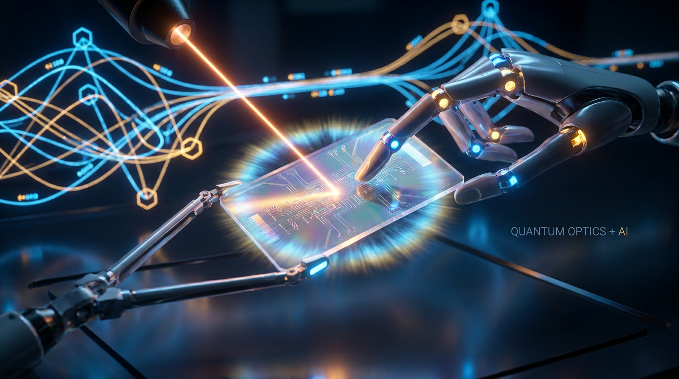
A landmark paper published in Nature has demonstrated a general-purpose artificial intelligence vision system that embeds core computer-vision operations directly into a light-manipulating planar material known as an optical metasurface. Rather than waiting for a camera sensor to digitize an image and send it to a graphics processing unit (GPU), this prototype processes the visual information as the light waves pass through the lens itself. The result is accurate, real-time perception that requires a fraction of the energy used by conventional on-device vision intelligence.[1]
To understand how this works, one must look closely at the metasurface—a two-dimensional artificial structure thinner than a human hair. The surface is studded with millions of subwavelength "meta-atoms," often consisting of crystalline silicon nanopillars just 300 nanometers thick. When light hits these microscopic pillars, its phase, amplitude, and polarization are altered in highly specific ways. By carefully engineering the geometry and arrangement of these pillars, researchers can force the incoming light waves to perform mathematical operations, such as the convolutions used in neural networks.[4][5]
In traditional machine vision, a convolutional neural network (CNN) applies digital filters to an image to detect edges, textures, and shapes. This requires moving massive amounts of data back and forth between a processor and memory—a structural limitation known as the von Neumann bottleneck. Optical computing bypasses this entirely. The metasurface acts as a physical, analog convolution kernel. As the light from an object passes through the engineered glass, the optical interference patterns automatically extract the necessary features before the light even hits a digital sensor.[4][6]

The efficiency gains of this approach are staggering. Recent research published in eLight showcased a hybrid system that loads over 99.99 percent of the computational burden onto a passive optical metasurface. Because the light does all the heavy lifting instantaneously, the system only requires a remarkably small digital backend—containing just a few hundred to a few thousand trainable parameters—to finalize the classification of the image.[2]
This hybrid architecture solves one of the most persistent challenges in optical computing: adaptability. Historically, optical chips had to be physically re-manufactured to perform a different task. However, by pairing a fixed, ultra-wide optical neural network with a compact digital backend, researchers can adapt the system to new tasks without retraining or re-fabricating the metasurface. The training time for such a network drops from tens of hours on a traditional GPU cluster to mere seconds, or even milliseconds if high-speed spatial light modulators are utilized.[2]
Performance metrics for these optical systems are already rivaling state-of-the-art digital models. In experimental trials, optical convolution systems have achieved 98.6 percent classification accuracy on standard handwritten digit datasets, and nearly 89 percent accuracy on more complex fashion image datasets. They maintain this high accuracy while remaining tolerant to fabrication imperfections and slight misalignments, proving that the technology is robust enough for real-world deployment.[2][4]

Performance metrics for these optical systems are already rivaling state-of-the-art digital models.
The implications for edge computing—devices that process data locally rather than relying on the cloud—are profound. Autonomous vehicles, for instance, must process high-resolution video streams in real time to navigate safely. Current digital systems require bulky, power-intensive computers in the trunk of the car. An optical metasurface could perform the initial feature extraction passively, drastically reducing the latency and power requirements of the vehicle's onboard AI.[5][6]
Similarly, the aerospace and drone industries stand to benefit immensely. Photonics Spectra recently highlighted how deliberately introducing "controlled chaos" into disordered mosaic metasurfaces allows multiple optical functions to be performed simultaneously within a single, compact footprint. For a lightweight drone, where every gram of payload and every milliwatt of battery life dictates operational limits, replacing a heavy digital processor with a weightless optical lens could exponentially increase flight times and capabilities.[3]
The medical field is also eyeing this technology for next-generation diagnostics. Endoscopes and biomedical imaging devices equipped with metasurfaces could perform real-time, high-contrast tissue analysis during surgery without the lag associated with digital processing. Because the optical computation happens instantaneously as the light reflects off the tissue, surgeons could receive immediate AI-assisted overlays highlighting potential malignancies.[3][4]
Crucially, the manufacturing pathway for these optical chips is already well-established. The silicon nanopillars used in these metasurfaces are fabricated using standard electron-beam lithography and reactive-ion etching—the exact same processes used by the global semiconductor industry to make traditional computer chips. This compatibility with existing CMOS (complementary metal-oxide-semiconductor) foundries means that scaling up production of optical AI chips does not require inventing entirely new manufacturing supply chains.[4][6]
Despite the rapid progress, challenges remain before optical computing completely replaces digital GPUs for vision tasks. Current metasurfaces are highly optimized for specific wavelengths and polarizations of light, making them somewhat sensitive to natural, incoherent lighting environments. Researchers are actively exploring dispersion engineering and spatial multiplexing to create broadband metasurfaces that can operate flawlessly in everyday sunlight.[4][5]
Furthermore, while optical systems excel at linear operations like convolutions, neural networks also require non-linear activation functions to make complex decisions. Currently, these non-linear steps are mostly handled by the digital backend. The race is now on to develop fully optical non-linear materials that can be integrated directly into the metasurface, paving the way for deep, multi-layered optical neural networks that operate entirely in the photonic domain.[5][6]
The bidirectional convergence of artificial intelligence and nanophotonics is creating a virtuous cycle. AI algorithms are now being used to inversely design the complex geometries of the metasurfaces themselves, discovering optimal nanopillar arrangements that human engineers could never deduce manually. In turn, these AI-designed optical chips provide the hardware acceleration needed to run even more advanced AI models.[5]

As the physical limits of Moore's Law loom over traditional silicon electronics, the shift toward light-based computing offers a vital escape route. By reimagining the camera lens not just as a window, but as a high-speed, zero-energy computer, the tech industry is laying the groundwork for a future where artificial intelligence is limited only by the speed of light.[1][6]
How we got here
Early 2020s
Researchers begin demonstrating that subwavelength metasurfaces can manipulate light to perform basic mathematical equations.
December 2024
Scientists successfully train arbitrarily shaped analog convolution kernels using optical metasurfaces, proving viability for machine vision.
March 2026
A hybrid architecture is published in eLight, showing that fixed optical front-ends can offload 99.99% of compute from digital backends.
April 2026
Engineers at Monash University unveil 'disordered mosaic metasurfaces' that integrate 11 distinct optical functions into a single device.
June 2026
Nature publishes a landmark paper on a general-purpose AI vision system embedded entirely within a light-manipulating planar material.
Viewpoints in depth
Photonic Engineers
Focus on the hardware breakthrough of manipulating light at the nanoscale to overcome the physical limits of traditional silicon transistors.
For hardware engineers, the metasurface represents an escape hatch from the looming death of Moore's Law. As traditional silicon transistors approach the size of individual atoms, making digital chips faster and more efficient has become exponentially difficult. Photonic engineers view metasurfaces as a fundamental shift in how computation is physically realized. By relying on the wave nature of light—specifically interference and diffraction—they can execute massive parallel computations instantly in free space. Their primary focus is on refining the geometry of the meta-atoms, utilizing AI-driven inverse design to discover nanopillar shapes that can manipulate multiple wavelengths and polarizations simultaneously, pushing the boundaries of what a passive piece of glass can calculate.
AI Software Developers
Value the hybrid architecture that offloads heavy mathematical convolutions to optics, drastically reducing model training times and digital compute loads.
From the software perspective, the appeal of optical computing lies in its ability to clear the von Neumann bottleneck. Training modern convolutional neural networks requires shuffling terabytes of data between memory and processors, a process that consumes massive amounts of time and electricity. AI developers are particularly enthusiastic about the hybrid models where the optical front-end is fixed, and only a tiny digital back-end needs to be trained. This architecture allows developers to adapt a vision system to a new task in seconds rather than hours. Their ongoing challenge is developing new training frameworks and algorithms that natively understand and optimize for the analog quirks of optical hardware, bridging the gap between digital code and photonic physics.
Edge Computing Advocates
Emphasize the practical applications for autonomous vehicles, drones, and medical devices where power, weight, and real-time processing are critical.
For industries building devices that operate in the real world, the primary constraints are always battery life, weight, and heat dissipation. Edge computing advocates see optical metasurfaces as the key to untethering advanced AI from the cloud. An autonomous drone cannot carry a liquid-cooled GPU server, nor can it rely on a cellular connection to process video feeds when flying in remote areas. By replacing heavy digital processors with weightless, zero-energy optical lenses, manufacturers can build smarter, faster-reacting machines. This camp is pushing for the rapid commercialization of the technology, focusing on integrating these metasurfaces into standard camera modules for robotics, augmented reality headsets, and biomedical endoscopes.
What we don't know
- How effectively these optical systems will perform in highly variable, natural lighting conditions outside of controlled laboratory environments.
- The timeline for integrating fully optical non-linear activation functions, which would eliminate the need for the digital backend entirely.
- How quickly traditional semiconductor foundries will pivot to mass-producing these specific metasurface architectures at commercial scale.
Key terms
- Metasurface
- A two-dimensional, artificially engineered material with subwavelength structures designed to control and manipulate electromagnetic waves.
- Convolutional Neural Network (CNN)
- A type of artificial intelligence algorithm commonly used for analyzing visual imagery by applying mathematical filters to detect features like edges and shapes.
- Von Neumann Bottleneck
- A limitation in traditional computer architecture where processing speed is restricted by the time it takes to move data back and forth between the processor and memory.
- Nanophotonics
- The study and application of light behavior on the nanometer scale, often involving the interaction of light with microscopic structures.
- Edge Computing
- Processing data locally on the device where it is generated (like a drone or car), rather than sending it to a centralized cloud server.
Frequently asked
What is an optical metasurface?
It is an ultra-thin, flat material covered in microscopic structures (like silicon nanopillars) that manipulate the phase, amplitude, and polarization of light passing through it.
How does this save energy compared to normal AI?
Traditional AI requires converting light into digital data and running it through power-hungry computer chips. Optical computing performs the math using the light waves themselves, requiring zero electricity for that portion of the calculation.
Can this completely replace digital computer chips?
Not yet. Current systems use a 'hybrid' approach where the optical lens does 99% of the heavy lifting, but a small digital chip is still needed at the end to finalize the AI's decision.
When will this technology be used in the real world?
Prototypes are already achieving high accuracy in lab settings. Because the chips can be made using standard semiconductor manufacturing techniques, commercial applications in drones and medical devices could emerge in the near future.
Sources
Source coverage
6 outlets
3 viewpoints surfaced


[1]NaturePhotonic Engineers
Reimagining machine vision with optical computing
Read on Nature →[2]eLightPhotonic Engineers
Highly scalable machine vision enabled with meta-optics-based ultra-wide neural network
Read on eLight →[3]Photonics SpectraEdge Computing Advocates
Mosaic Metasurface Design Allows Multifunctionality in Optical Devices
Read on Photonics Spectra →[4]ACSAI Software Developers
Spatial frequency domain training method to create arbitrarily shaped analog convolution kernels
Read on ACS →Artificial intelligence with metasurfaces: from intelligent design to intelligent computing
Read on PhotoniX →[6]Factlen Editorial Team
Synthesis by Factlen editorial team
Read on Factlen Editorial Team →


Every angle. Every day.
Get science stories with full source coverage and perspective breakdowns delivered to your inbox.