How Glass Substrates Are Breaking the AI Chip Packaging Bottleneck
The semiconductor industry is shifting from traditional plastic to glass substrates to prevent massive AI chips from warping under extreme heat, unlocking the next generation of computing power.
By Factlen Editorial Team
- Foundry & IDM Giants
- Leading chipmakers view glass as the necessary evolution to sustain Moore's Law for AI workloads.
- Materials & Equipment Innovators
- Supply chain companies focus on the chemical and mechanical breakthroughs required to handle glass at scale.
- Display Manufacturers
- Traditional panel makers see an opportunity to pivot their glass expertise into the high-margin semiconductor space.
What's not represented
- · Environmental impact analysts assessing the energy cost of glass fabrication
- · Consumer electronics brands waiting for cost reductions
Why this matters
The exponential growth of artificial intelligence is currently bottlenecked by the physical limitations of the plastics used to package chips. By transitioning to glass, the semiconductor industry is unlocking the next decade of computing power, enabling the massive, ultra-fast processors required for future AI, 6G networks, and autonomous systems.
Key points
- Traditional plastic chip substrates are warping under the extreme heat generated by modern AI accelerators.
- Glass substrates match the thermal expansion of silicon, keeping the package perfectly flat at high temperatures.
- Lasers can drill microscopic holes in glass, allowing for significantly denser electrical connections than plastic.
- Intel, TSMC, and Samsung are investing billions to bring glass packaging to mass production by the end of the decade.
- Display manufacturers are pivoting their TV-glass expertise to enter the lucrative semiconductor supply chain.
- The primary hurdle remains the brittleness of glass, requiring entirely new robotic handling systems in fabrication plants.
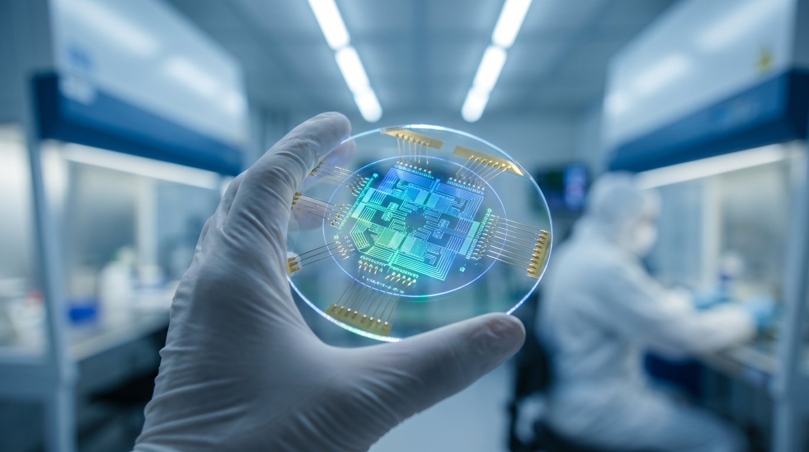
For decades, the semiconductor industry has relied on a quiet workhorse to connect microscopic silicon brains to the outside world: organic substrates. These small squares of plastic and woven fiberglass sit beneath the chip, routing electrical signals and power. But as artificial intelligence models demand increasingly massive, power-hungry processors, this foundational material is reaching its physical breaking point. To keep the AI revolution moving, the world’s largest chipmakers are turning to a material that is simultaneously ancient and cutting-edge: glass.[1][3]
The transition to glass substrates represents one of the most significant shifts in semiconductor packaging in a quarter-century. Industry giants including Intel, TSMC, and Samsung are currently pouring billions of dollars into the technology, racing to overcome manufacturing hurdles and bring glass-packaged chips to mass production. The stakes are immense; the company that masters glass packaging first will likely dictate the pace of AI hardware scaling for the next decade, unlocking capabilities in high-performance computing, 6G communications, and autonomous mobility that are currently constrained by physical bottlenecks.[1][2]
To understand why glass is necessary, one must look at the limitations of current advanced packaging. Modern AI accelerators are not single chips; they are "chiplets"—multiple processors and high-bandwidth memory modules stitched together on a single package. As these packages grow larger to accommodate more compute power, they generate immense heat. Organic materials expand at a rate of 17 to 20 parts per million per degree Celsius, while the silicon chips attached to them expand at just 3 parts per million.[1][6]
This coefficient of thermal expansion (CTE) mismatch creates a severe mechanical problem known as warpage. When an AI chip heats up under heavy workloads, the plastic substrate expands faster than the silicon, causing the entire package to bend. On massive AI accelerators, this warpage degrades performance, breaks microscopic connections, and drastically reduces manufacturing yields. Glass, however, can be chemically engineered to have a thermal expansion rate nearly identical to silicon, virtually eliminating the warpage problem even as package sizes continue to balloon.[3][5]

Beyond thermal stability, glass solves a critical density bottleneck. In traditional organic substrates, the vertical connections that route signals between layers—known as vias—are created using mechanical drills, which limits their minimum diameter to roughly 100 micrometers. Glass substrates, by contrast, utilize Through-Glass Vias (TGVs). Because glass is exceptionally flat and structurally rigid, manufacturers can use precision lasers and chemical etching to drill TGVs as small as 10 to 30 micrometers.[1][6]
This microscopic precision allows engineers to pack vastly more connections into the same physical footprint. It also enables redistribution layers (RDLs) with wiring spaces smaller than two micrometers, a density that organic cores simply cannot support. For AI workloads, where data must travel between the graphics processing unit (GPU) and high-bandwidth memory at blistering speeds, this increased interconnect density is the difference between a system that bottlenecks and one that flows freely.[6][8]
The electrical properties of glass offer another massive advantage for the future of computing. Glass is an excellent insulator with a very low dielectric constant and low tangent loss. In practical terms, this means electrical signals traveling through glass experience significantly less degradation and signal loss compared to organic materials or silicon interposers. Intel has already demonstrated signal integrity of 448 gigabits per second on glass substrates, proving the material's viability for the ultra-high-frequency demands of next-generation data centers and 6G networks.[1][6]
The electrical properties of glass offer another massive advantage for the future of computing.
Furthermore, the optical transparency of glass opens the door to a holy grail of semiconductor design: co-packaged optics. As electrical signals struggle to keep up with data demands, the industry is moving toward using light (photonics) to transmit data between chips. Glass substrates provide an ideal medium for embedding optical waveguides directly into the package, allowing light to travel seamlessly alongside electrical pathways. This hybrid approach promises to dramatically reduce latency and power consumption in massive AI server farms.[5][6]

Recognizing these physical imperatives, the race to commercialize glass substrates has accelerated from laboratory research to factory construction. Intel has been the most vocal pioneer, committing over $1 billion to glass substrate research and development. At the NEPCON Japan exhibition in early 2026, Intel showcased a massive 78-by-77-millimeter sample that successfully integrated its advanced packaging technology with a thick glass core, achieving a flawless structure with no micro-cracks. The company expects its glass substrate products to see widespread deployment between 2026 and 2030.[1][3][7]
TSMC, the world's dominant foundry, is aggressively pursuing its own glass-based solutions to maintain its grip on the AI chip market. The Taiwanese giant recently unveiled its CoPoS (Chip-on-Panel-on-Substrate) product line, which utilizes a glass interposer rather than a full glass core. TSMC plans to establish a mini production line in 2026, transition to small-volume trial production by 2027, and reach full mass production by 2028 or 2029. This timeline aligns closely with the anticipated release of next-generation AI architectures that will require larger-than-reticle packaging.[3][7]
Meanwhile, the South Korean semiconductor ecosystem is mobilizing rapidly. SK Absolics, backed by funding from the U.S. CHIPS Act, is constructing a dedicated glass substrate manufacturing facility in Covington, Georgia, targeting mass production as early as 2026. Samsung is leveraging a vertically integrated strategy, drawing on the expertise of its semiconductor, electro-mechanics, and display divisions. Samsung Electro-Mechanics delivered its first glass substrate samples to a global Big Tech client in late 2025 and is officially targeting 2028 for mass integration into high-performance AI chipsets.[1][4]

The shift to glass has also created an unexpected opportunity for the display industry. Companies that have spent decades perfecting the mass production of ultra-thin, flawless glass panels for televisions and smartphones are now pivoting to semiconductors. Chinese display giant BOE Technology has established semiconductor glass substrates as a core corporate strategy, planning to leverage its depreciated panel production lines to achieve mass production by 2027. Visionox and LG Innotek are making similar moves, hoping to capture high-margin semiconductor revenue as the traditional display market matures.[4][7]
Despite the immense promise and capital flowing into the sector, significant manufacturing hurdles remain. The most obvious challenge is the inherent brittleness of glass. Semiconductor fabrication plants are highly automated environments where silicon wafers are rapidly spun, baked, and transported by robotic arms. Introducing ultra-thin glass panels into these high-stress environments requires entirely new handling protocols and equipment to prevent catastrophic shattering on the production line.[3][4]
The equipment ecosystem is currently undergoing a massive overhaul to support the glass transition. Companies like LPKF are developing specialized laser systems for TGV drilling, while Lam Research and Applied Materials are adapting their etching and plating tools for glass chemistry. Inspection tools from KLA and Onto Innovation must be recalibrated, as the transparency and reflective properties of glass confuse optical sensors designed to scan opaque silicon and organic materials.[3][6]

As the industry pushes through these growing pains, 2026 is emerging as the critical inflection point where glass substrates transition from a promising research concept to a commercial reality. While they will initially be reserved for the most expensive, high-margin AI accelerators and data center switches, the technology is expected to eventually trickle down to consumer electronics. By breaking the thermal and density bottlenecks of organic plastics, glass is ensuring that the exponential growth of computing power can continue unabated into the next decade.[7][8]
How we got here
Sept 2023
Intel officially commits to glass substrates in its advanced packaging roadmap.
Late 2025
Samsung Electro-Mechanics delivers its first glass substrate samples to global Big Tech clients.
Jan 2026
Intel debuts a massive 78x77mm glass core sample with zero micro-cracks at NEPCON Japan.
2026
SK Absolics targets the start of mass production at its new facility in Georgia.
2028-2029
TSMC and Samsung target full mass production of their glass-based packaging solutions.
Viewpoints in depth
Foundry & IDM Giants
Leading chipmakers view glass as the necessary evolution to sustain Moore's Law for AI workloads.
Companies like Intel, TSMC, and Samsung argue that organic substrates have reached their physical limits. For these giants, glass is not just an alternative material; it is a fundamental requirement to keep scaling AI accelerators. They point to the severe warpage issues and interconnect density limits of plastics as hard barriers to future performance, justifying their billion-dollar investments in glass R&D despite the immense manufacturing challenges.
Materials & Equipment Innovators
Supply chain companies focus on the chemical and mechanical breakthroughs required to handle glass at scale.
For equipment manufacturers and materials scientists, the glass transition is primarily a mechanical challenge. They emphasize that while the electrical properties of glass are superior, its brittleness requires an entirely new fabrication ecosystem. This camp is focused on developing precision laser drilling for Through-Glass Vias (TGVs), specialized chemical etching, and novel robotic handling systems that can move ultra-thin glass panels through a fab without catastrophic shattering.
Display Manufacturers
Traditional panel makers see an opportunity to pivot their glass expertise into the high-margin semiconductor space.
Companies with deep roots in LCD and OLED manufacturing, such as BOE and Visionox, view the shift to glass substrates as a rare opportunity to enter the lucrative semiconductor supply chain. They argue that their decades of experience in handling, cutting, and processing massive, flawless glass panels gives them a unique advantage over traditional semiconductor packaging firms, allowing them to repurpose depreciated display factories for next-generation chip packaging.
What we don't know
- Whether the equipment ecosystem can scale fast enough to meet the 2028 mass production targets without severe yield issues.
- Exactly how much of a price premium glass-packaged AI chips will carry over traditional organic packages.
- Which specific glass chemistry (borosilicate, fused silica, or synthetic quartz) will become the ultimate industry standard.
Key terms
- Substrate
- The foundational base layer that physically supports a microchip and connects its microscopic wiring to the main circuit board.
- Organic Substrate
- The traditional chip packaging material used for the last 25 years, made from a blend of plastics and woven fiberglass.
- Through-Glass Via (TGV)
- Microscopic vertical holes drilled into a glass substrate using lasers, allowing electrical signals to pass through the material.
- Coefficient of Thermal Expansion (CTE)
- A scientific measurement of how much a material expands or shrinks when exposed to changes in temperature.
- Warpage
- The physical bending or bowing of a chip package that occurs when different materials (like silicon and plastic) expand at different rates under heat.
- Co-packaged Optics
- An advanced technology that uses light (photonics) instead of electricity to transmit data between chips, which glass substrates help enable.
Frequently asked
Why are chipmakers switching from plastic to glass?
As AI chips grow larger and run hotter, traditional plastic (organic) substrates warp and bend. Glass has a thermal expansion rate identical to silicon, meaning it stays perfectly flat under extreme heat, preventing damage to the chip.
Will glass substrates make computers cheaper?
Initially, no. Glass packaging will first be used in high-end, expensive AI accelerators and data center servers. However, as the technology matures, it could lower costs by replacing expensive silicon interposers.
Isn't glass too fragile for semiconductor manufacturing?
Brittleness is the biggest challenge. The industry is currently developing specialized robotic handling systems, low-stress chemical etching, and precision lasers to process ultra-thin glass panels without shattering them on the production line.
When will glass-packaged chips be widely available?
Small-scale trial production is beginning in 2026, with major foundries like TSMC, Intel, and Samsung targeting widespread mass production between 2028 and 2030.
Sources
Source coverage
8 outlets
3 viewpoints surfaced


[1]PandailyFoundry & IDM Giants
Glass Substrates Set to Reshape Semiconductor Packaging as Industry Giants Pour Billions Into Technology
Read on Pandaily →[2]SCHOTTMaterials & Equipment Innovators
Beyond speed: what glass-based chips mean for the devices of tomorrow
Read on SCHOTT →[3]TrendForceFoundry & IDM Giants
Glass Substrates Are Breaking Through the AI Chip Packaging Bottleneck
Read on TrendForce →[4]The EconomyFoundry & IDM Giants
AI Packaging Game-Changer 'Glass Substrates' Ignite Global Race Toward Mass Production
Read on The Economy →[5]AT&SMaterials & Equipment Innovators
Glass Core Substrates: From R&D breakthrough to platform technology
Read on AT&S →[6]Semiconductor EngineeringMaterials & Equipment Innovators
Glass Substrates Gain Momentum
Read on Semiconductor Engineering →[7]36KrDisplay Manufacturers
Glass Substrates: The Dark Horse in 2026
Read on 36Kr →[8]MDPIMaterials & Equipment Innovators
A Review of Glass Substrate Technologies
Read on MDPI →

More in technology
See all 51 stories →Algorithmic Choice
The Era of Algorithmic Choice: How User-Controlled Feeds are Rewiring Social Media
8 sources
Battery Tech
Solid-State Batteries Move From Lab to Road, Promising 1,000-Kilometer EV Ranges
7 sources
Atmospheric Water Harvesting
Engineers Develop a Wearable Jacket That Harvests Drinking Water Directly From the Air
6 sources

AI Scaffolding
Microsoft and Xiaomi Open-Source Breakthroughs in AI Coding Memory and Skills
8 sources

Every angle. Every day.
Get technology stories with full source coverage and perspective breakdowns delivered to your inbox.