How Photonic Chips Are Using Light to Solve AI's Energy Crisis
As artificial intelligence pushes the physical limits of traditional silicon, a new generation of processors is replacing electricity with light. Photonic accelerators promise to perform complex AI computations at near-zero energy, offering a sustainable path forward for the tech industry.
By Factlen Editorial Team
- Photonic Hardware Developers
- Advocates for native optical computing to replace silicon bottlenecks.
- Silicon Incumbents
- Proponents of hybrid architectures and optical interconnects.
- Energy & Climate Analysts
- Stakeholders focused on the macroeconomic impact of AI power demand.
What's not represented
- · Foundry Operators
- · Software Developers
Why this matters
The exponential growth of AI is currently on a collision course with global electricity limits. By transitioning from electrons to photons, the tech industry can continue to scale AI capabilities without overwhelming power grids or derailing climate goals.
Key points
- AI models are consuming unsustainable amounts of electricity, pushing traditional silicon chips to their physical and thermal limits.
- Photonic accelerators solve this by using particles of light (photons) instead of electricity to perform complex mathematical calculations.
- Because light travels without electrical resistance, optical chips can operate with up to 100 times the energy efficiency of standard GPUs.
- The technology allows multiple data streams to be processed simultaneously using different colors of light, massively increasing computing speed.
- While fully optical computers are still years away, hybrid chips combining silicon memory with photonic processors are already entering data centers.
The artificial intelligence industry is currently on a collision course with the fundamental laws of physics. As large language models and generative AI systems scale to unprecedented sizes, their appetite for electricity has surged to levels that threaten to overwhelm global power grids. Data centers, once quiet warehouses of servers, are now industrial-scale power consumers, drawing gigawatts of energy just to keep their processors running. For the industry to continue advancing without causing an energy crisis, a radical shift in hardware architecture is urgently required.[4]
For decades, the technology world relied on Moore’s Law—the steady shrinking of transistors to pack more computing power into the same silicon footprint. But that era is rapidly approaching its physical limits. When electrons are forced through increasingly microscopic copper wires, they face electrical resistance. This resistance generates massive amounts of heat, which in turn requires even more power to cool the systems down. The industry refers to this as the "power wall," and traditional electronic chips are hitting it at full speed.[3]
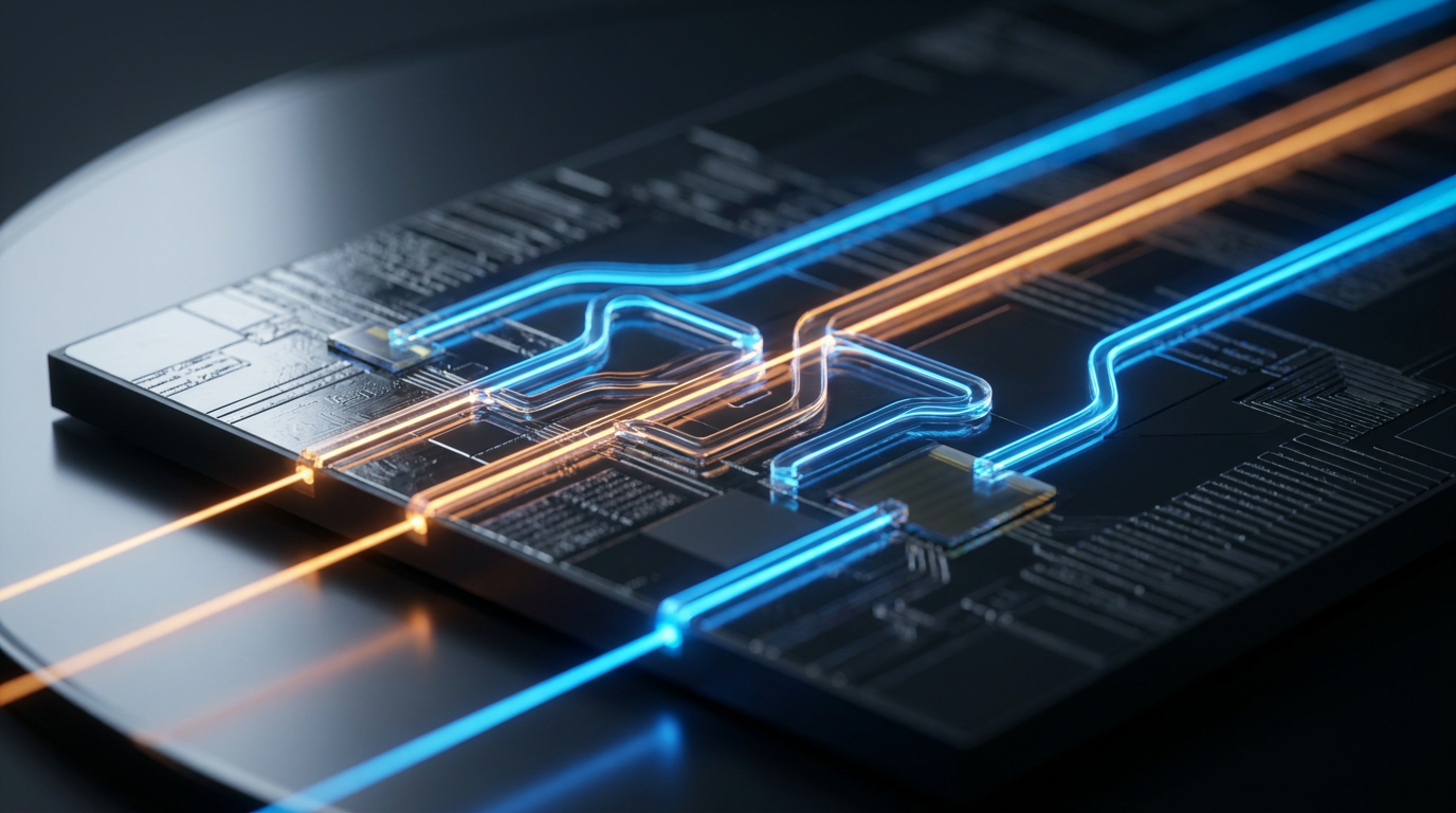
Enter photonic computing. Instead of relying on electrons crawling through metal wires, a new generation of AI accelerators uses photons—particles of light—to process and transmit data. By harnessing the unique physical properties of light, these chips promise to bypass the thermal and electrical bottlenecks of traditional silicon. The concept of using light for data transmission is not entirely new; fiber-optic cables have formed the high-speed backbone of the global internet for decades. However, once those optical signals reach a data center, they hit a critical bottleneck. The light must be converted back into electrons for the processor to perform its mathematical operations, erasing many of light's inherent advantages and adding severe latency and energy costs.[5][6]

Photonic AI chips eliminate this costly conversion step entirely. They are designed to perform the actual mathematical calculations natively in light. Specifically, they excel at matrix multiplications—the complex, repetitive linear algebra operations that form the foundational bedrock of all deep neural networks. By processing these calculations optically, the chip operates at the literal speed of light. The mechanism behind this breakthrough relies on microscopic optical components etched directly into standard silicon wafers. Lasers are used to generate the light, while microscopic channels known as waveguides steer the beams across the chip. Modulators then encode digital data by subtly altering the light's physical properties, such as its phase or amplitude, before photodetectors read the final computational results.[3][5]
At the heart of many of these optical architectures are devices called Mach-Zehnder interferometers (MZIs). These microscopic structures split a single beam of light into two separate paths, alter the phase of one path, and then recombine them. The resulting interference pattern naturally and instantly performs the mathematical multiplication required by AI algorithms, requiring zero electrical logic gates. Another highly promising approach utilizes miniature Fresnel lenses. Researchers at the University of Florida recently demonstrated a prototype chip that uses these microscopic, lighthouse-style lenses to perform convolutions. Convolutions are the core pattern-finding operations essential for machine learning tasks like image classification, facial recognition, and advanced video processing.[2][5][7]
At the heart of many of these optical architectures are devices called Mach-Zehnder interferometers (MZIs).
The performance gains offered by these optical mechanisms are staggering. Because photons have no mass and no electrical charge, they do not bump into each other or experience resistance the way electrons do. They glide seamlessly through the chip's waveguides without generating the thermal friction that plagues traditional graphics processing units (GPUs). This lack of friction translates directly to unprecedented energy efficiency. Studies indicate that in traditional electronic AI chips, up to 80 percent of the consumed energy is wasted simply shuttling data back and forth between the processor and the memory banks. The actual computation accounts for only a fraction of the power draw. Light elegantly solves this massive data-movement crisis.[5][6]

By computing and transmitting with light, photonic accelerators can operate with 10 to 100 times the efficiency of current silicon chips. In rigorous tests, the University of Florida's optical convolution chip achieved 98 percent accuracy on handwritten digit classification tasks—matching the performance of traditional hardware—while consuming near-zero energy for the core mathematical computation. Speed is the other major advantage of the photonic approach. An electronic transistor has a hard physical limit to how fast it can switch on and off to process binary data. Light bypasses this switching delay entirely. The calculation happens continuously as the light flows through the physical structure of the chip, offering a paradigm shift in processing velocity.[2][7]
A team of scientists at MIT recently unveiled a fully integrated photonic processor capable of running a deep neural network classification task in less than half a nanosecond. This near-instantaneous processing opens the door to real-time AI applications where milliseconds matter, such as autonomous vehicle navigation, high-speed telecommunications, and advanced scientific research. Furthermore, light offers a unique physical property called wavelength-division multiplexing. Unlike electrons, which must travel single-file through a copper wire to avoid scrambling the signal, multiple distinct colors—or wavelengths—of light can travel through the exact same optical waveguide simultaneously without interfering with one another.[1][5]

This multiplexing capability allows a single photonic chip to process multiple data streams in parallel. By simply adding more colors of laser light to the system, engineers can multiply the chip's computational throughput without increasing its physical footprint or significantly raising its power draw—a feat impossible in the electronic realm. The transition from academic laboratories to commercial data centers is already well underway. Startups like Lightmatter and Ayar Labs have raised hundreds of millions of dollars to bring optical AI hardware to market. Lightmatter’s Envise processor, for example, integrates photonic tensor cores to handle massive deep learning workloads at a fraction of the power cost of traditional server racks.[3][5]
Meanwhile, traditional silicon giants like NVIDIA, Intel, and Broadcom are heavily investing in co-packaged optics and optical interconnects. Rather than attempting to replace the entire GPU immediately, they are using light to bridge the communication gaps between existing electronic chips, solving the massive data-transfer bottleneck that currently throttles supercomputers. Despite the immense momentum, optical computing still faces significant engineering hurdles. Photonic components are fundamentally limited by the physical wavelength of light, making them substantially larger than modern nanoscale electronic transistors. Achieving the extreme packing density seen in modern CPUs remains a formidable manufacturing challenge for the industry.[4][6]

Additionally, optical systems are highly sensitive to microscopic temperature fluctuations, and creating efficient photonic memory to store light-based data long-term is still an unsolved puzzle. For the foreseeable future, the industry will rely on hybrid architectures—using electronics for memory storage and logic control, while deploying photonics for heavy matrix math and rapid data transfer. Ultimately, the shift toward light-based computing represents a fundamental departure from the silicon status quo that has defined the digital age. As artificial intelligence models continue their exponential growth, photonic accelerators offer a sustainable, high-performance path forward, ensuring that the next generation of AI is constrained only by human ingenuity, rather than the limits of the power grid.[4][6]
How we got here
1980s-1990s
Fiber-optic cables become the standard for long-distance internet data transmission.
2015
Startups like Ayar Labs are founded to bring optical data transfer directly to computer chips.
2023
Major investments flow into photonic AI startups as the energy demands of large language models become apparent.
2024
MIT researchers demonstrate a fully integrated optical neural network capable of sub-nanosecond processing.
2025
The University of Florida unveils a near-zero energy optical chip using Fresnel lenses for AI image recognition.
Viewpoints in depth
Photonic Hardware Developers
Advocates for native optical computing to replace silicon bottlenecks.
Researchers and startups in the photonics space argue that the tech industry has reached the physical limits of Moore's Law. They believe that continuing to scale AI with traditional silicon will result in unsustainable energy consumption and thermal throttling. By processing matrix multiplications natively in light, they assert that the industry can achieve orders-of-magnitude improvements in both speed and efficiency, fundamentally altering the trajectory of AI hardware.
Silicon Incumbents
Proponents of hybrid architectures and optical interconnects.
Established chipmakers acknowledge the power of light but view it through a pragmatic lens. Rather than discarding decades of electronic computing infrastructure, they advocate for hybrid approaches. Their immediate focus is on 'co-packaged optics'—using light to shuttle data between traditional GPUs at massive speeds. They point out that optical memory remains a significant hurdle, making all-photonic chips impractical for general-purpose computing in the near term.
Energy & Climate Analysts
Stakeholders focused on the macroeconomic impact of AI power demand.
For grid operators and climate scientists, the AI boom represents a looming energy crisis. They view photonic computing not just as a performance upgrade, but as a necessary climate intervention. With AI data centers projected to consume a massive share of global electricity by 2050, these analysts argue that adopting ultra-efficient optical hardware is essential to meeting international renewable energy targets and preventing grid failures.
What we don't know
- How quickly semiconductor foundries can scale up the manufacturing of microscopic optical components to meet global demand.
- Whether researchers can successfully develop 'photonic memory' to store data in light, which remains a major technical hurdle.
- How the cost of optical AI accelerators will compare to traditional silicon GPUs once mass production begins.
Key terms
- Photonic Integrated Circuit (PIC)
- A microchip that uses light instead of electricity to process and transmit information.
- Mach-Zehnder Interferometer (MZI)
- An optical device that splits a beam of light and recombines it to perform mathematical calculations based on how the light waves interfere.
- Waveguide
- A microscopic pathway etched into a chip that steers and directs light, functioning like a wire for photons.
- Convolution
- A fundamental mathematical operation in AI used to detect patterns, edges, and features in images and video.
- Co-packaged Optics
- A design approach that places optical communication components on the same package as the electronic processor to speed up data transfer.
Frequently asked
What is a photonic AI accelerator?
It is a computer chip that uses particles of light (photons) instead of electricity (electrons) to perform the heavy mathematical calculations required for artificial intelligence.
Why is computing with light more efficient?
Unlike electrons, photons have no mass or electrical charge, meaning they travel without resistance. This eliminates the massive heat generation and energy loss associated with traditional silicon chips.
Can optical chips replace my computer's CPU?
Not in the near future. Photonic chips excel at specific AI tasks like matrix multiplication, but traditional electronic CPUs are still better suited for general-purpose logic and memory storage.
What is wavelength-division multiplexing?
It is a technique where multiple different colors of light are sent through the same optical pathway simultaneously, allowing the chip to process many data streams at once without interference.
Sources
Source coverage
7 outlets
3 viewpoints surfaced


[1]MIT NewsPhotonic Hardware Developers
Scientists develop a new photonic chip that overcomes roadblocks
Read on MIT News →[2]University of FloridaPhotonic Hardware Developers
New computer chip uses light instead of electricity for AI
Read on University of Florida →[3]LightmatterPhotonic Hardware Developers
A New Kind of Computer
Read on Lightmatter →[4]Science|BusinessEnergy & Climate Analysts
HAETAE project building processors to resolve future AI bottlenecks
Read on Science|Business →[5]FindLightPhotonic Hardware Developers
Photonic AI accelerators use light instead of electrons
Read on FindLight →[6]Factlen Editorial TeamSilicon Incumbents
Synthesis by Factlen editorial team
Read on Factlen Editorial Team →[7]SPIEPhotonic Hardware Developers
Silicon chip uses light with electricity to perform convolution operations
Read on SPIE →
Every angle. Every day.
Get ai stories with full source coverage and perspective breakdowns delivered to your inbox.