The Invisible Revolution: Why the Semiconductor Industry is Swapping Plastic for Glass
As AI chips grow too hot and complex for traditional organic materials, the semiconductor industry is racing to adopt glass core substrates. This breakthrough promises to unlock the next decade of computing power by drastically increasing wiring density and thermal stability.
By Factlen Editorial Team
- Foundries & Chip Designers
- Focus on overcoming the physical limits of organic substrates to enable next-generation AI processors.
- Materials & Equipment Suppliers
- Focus on solving the manufacturing, handling, and laser-drilling challenges of working with ultra-thin glass.
- Industry Analysts
- Track the commercial viability, yield rates, and market growth of the emerging glass packaging sector.
What's not represented
- · Environmental Impact Analysts
- · Consumer Electronics Manufacturers
Why this matters
The physical limits of current chip packaging are threatening to stall the AI revolution. By transitioning to glass, engineers can pack significantly more computing power into data centers while reducing energy consumption, paving the way for more advanced and efficient AI models.
Key points
- AI chips have grown too large and hot for traditional plastic (organic) substrates to handle without warping.
- The industry is transitioning to glass core substrates, which offer superior thermal stability and rigidity.
- Glass allows for a 10x increase in wiring density through microscopic laser-drilled channels called Through-Glass Vias (TGV).
- The transparency of glass enables optical interconnects, allowing data to be transmitted via light to save energy.
- Major foundries like Intel and TSMC are racing to commercialize the technology between 2026 and 2028.
The artificial intelligence boom has a physical limit, and surprisingly, it isn't just the microscopic size of the transistors. For sixty years, the semiconductor industry worshipped Moore’s Law, relentlessly shrinking silicon gates to pack more computing power into every square millimeter. But as artificial intelligence models scale into the trillions of parameters, the physical chips required to train them have grown massive. The bottleneck is no longer just the silicon itself; it is the foundation that the silicon sits on.[7]
Today’s most advanced AI accelerators are no longer single, monolithic squares of silicon. Instead, they are sprawling "chiplet" architectures—complex jigsaw puzzles of logic processors and high-bandwidth memory stitched together into a single package. To function cohesively as a single brain, these individual chiplets must communicate with each other at lightning speed. This requires an incredibly dense network of microscopic wires to route power and data, a task that falls entirely on the packaging technology holding the components together.[1][7]
The critical bottleneck in this communication network lies in the foundation beneath the silicon. Every chip sits on a carrier board known as a substrate, which serves as the crucial bridge routing electrical signals and power between the microscopic world of the processor and the macroscopic world of the motherboard. Without a robust and highly conductive substrate, even the most advanced silicon processor is effectively stranded, unable to draw enough power or transmit its calculations to the rest of the system.[1]
For over two decades, the industry standard for this foundation has been the organic substrate, primarily relying on a specialized resin known as Ajinomoto Build-up Film (ABF). Organic substrates are essentially high-tech plastics. They have been wildly successful because they are relatively cheap, highly reliable, and easy to manufacture at scale. They have powered everything from smartphones to traditional data center servers. But in the era of hyperscale artificial intelligence, where chips draw unprecedented amounts of electricity, these plastic foundations are finally hitting an insurmountable physics wall.[1][6]

The primary problem is heat and physical space. Next-generation AI systems generate immense thermal loads during operation. When exposed to these extreme temperatures, organic materials naturally expand, warp, and bend. Imagine trying to build a towering skyscraper on a foundation made of flexible wood; eventually, as the structure grows heavier and the environment shifts, the foundation buckles. In a semiconductor package, even a microscopic warp in the substrate can misalign the delicate connections, leading to catastrophic failure.[1][3]
Furthermore, organic substrates severely limit how densely engineers can pack the microscopic wires connecting the chiplets. The industry is rapidly approaching the maximum physical size—known as the "reticle limit"—that an organic package can support before signal integrity degrades and power delivery fails. To build the next generation of AI supercomputers, engineers need a substrate that can span significantly larger areas without bending, while simultaneously supporting a much finer mesh of electrical routing to keep the data flowing.[1][7]
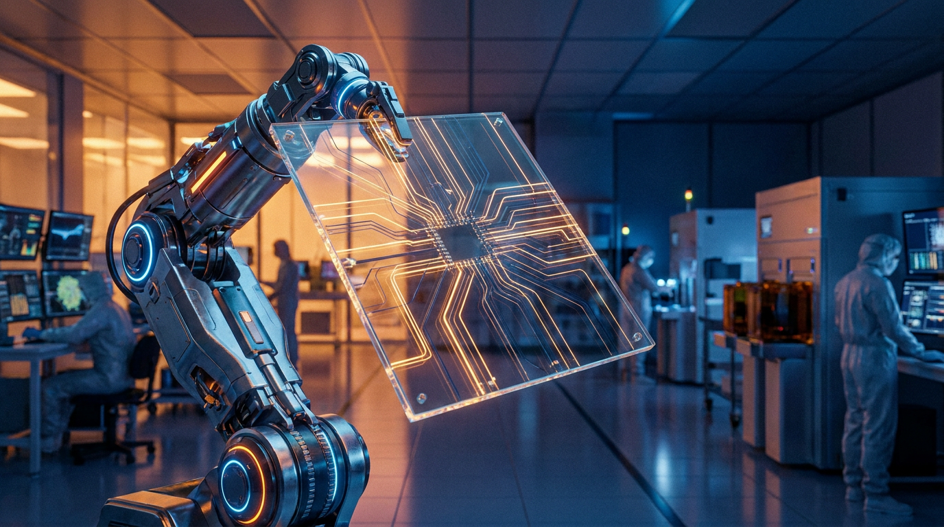
To keep the artificial intelligence revolution moving forward, the semiconductor industry is currently executing a radical materials pivot: swapping the plastic floor for glass. Known as glass core substrates, this emerging technology replaces the traditional organic resin core with specialized, ultra-flat glass. By fundamentally changing the material properties of the carrier board, chipmakers are unlocking a new paradigm in advanced packaging that promises to sustain the industry's exponential growth for another decade, bypassing the thermal limitations of plastic.[1][4]
Glass offers a suite of physical properties that seem almost tailor-made for the extreme demands of advanced computing. First and foremost, it possesses exceptional dimensional stability. Glass is highly rigid and barely expands or warps under intense heat, ensuring that the microscopic connections above it remain perfectly aligned regardless of the thermal load. This rigidity allows manufacturers to build significantly larger chip packages without the fear of the substrate buckling under the weight and heat of multiple processors.[3][4]
Second, glass enables a massive leap in wiring density through a specialized manufacturing technique called Through-Glass Vias (TGV). In traditional organic substrates, manufacturers must mechanically drill relatively wide holes through the plastic to connect different layers. With glass, manufacturers use precision lasers to bore microscopic, perfectly vertical channels through the core. These channels are then filled with conductive metal, creating ultra-fine pathways for electrical signals to travel between the chip and the board with unprecedented precision and minimal signal interference.[1][6]
Second, glass enables a massive leap in wiring density through a specialized manufacturing technique called Through-Glass Vias (TGV).
According to industry data, TGV technology allows for via pitches—the distance between the center of one hole and the next—of around 100 micrometers. This represents roughly a tenfold increase in density compared to the 325-micrometer limit typical of organic carriers. This exponential increase means that ten times more signal and power channels can be routed in the exact same physical footprint, completely eliminating the data bottlenecks that currently plague multi-chip architectures and allowing processors to communicate instantly.[7]

This newfound density is exactly what unlocks the next phase of chiplet design. With a stable glass foundation, chipmakers can pack up to 50% more silicon dies into a single package. It allows for larger overall package sizes, moving from the current 100-millimeter limits toward massive 120-millimeter or even panel-sized formats. This means future AI accelerators can feature vastly more high-bandwidth memory and logic cores integrated seamlessly into one unified system, drastically reducing the physical space required in data centers while simultaneously boosting total computational output.[5][7]
Beyond purely electrical routing, glass introduces a profound optical advantage for future data transmission. As data transmission speeds continue to increase, pushing electrical signals through copper wires generates too much heat and suffers from severe signal loss over distance. To combat this, the industry is moving toward Co-Packaged Optics (CPO), a paradigm where data is transmitted via light—photons—rather than electricity, directly from the chip package itself to the broader network infrastructure.[3]
Because glass is naturally transparent and features exceptionally low dielectric loss, it can integrate optical waveguides directly into the substrate. This seamless electrical-optical integration allows light to travel straight through the foundation of the chip. By replacing energy-hungry copper interconnects with integrated photonics, data centers can drastically reduce their overall power consumption while simultaneously increasing the bandwidth available to their most powerful artificial intelligence models, solving a critical energy crisis in the tech sector.[2][3]
The realization of these immense benefits has triggered a multi-billion-dollar race among the world’s top semiconductor foundries. Intel, which pioneered much of the early research into the material, is currently retrofitting its facilities in Arizona to serve as a dedicated glass substrate mass-production base. The company has publicly demonstrated fully functional prototypes and is aggressively targeting commercial readiness for its advanced packaging solutions between 2026 and 2027, viewing glass as a critical pillar in its strategy to regain foundry leadership.[4][6]

TSMC, the world’s largest contract chipmaker, is developing its own proprietary glass architecture dubbed CoPoS, which stands for Chip on Panel on Substrate. The Taiwanese manufacturing giant has already established a dedicated pilot line to refine the process. Industry analysts expect TSMC to achieve large-scale mass production by 2028, a timeline reportedly designed to support future generations of NVIDIA's most advanced AI accelerators and custom silicon designs that will require unprecedented substrate stability.[4][6]
Meanwhile, the broader supply chain is rapidly localizing and scaling to meet the anticipated demand. Absolics, a subsidiary of South Korea’s SKC, recently completed a massive manufacturing facility in Covington, Georgia. Backed by strategic funding from the U.S. CHIPS Act, the facility is already operational and shipping prototype glass substrates to major semiconductor clients like AMD, marking a significant step in establishing a robust domestic advanced packaging supply chain in North America.[2][7]
Materials giants are also pivoting their massive industrial capabilities toward the semiconductor sector. Corning, leveraging decades of expertise in fiber optics and display glass, has partnered with major panel makers like BOE to adapt flat-panel display manufacturing techniques to chip packaging. This 'panel-level' processing approach could eventually yield 300% more usable area per manufacturing run than traditional circular silicon wafers, drastically lowering the long-term cost of production and making the technology viable for a wider range of computing applications.[3][6]
Despite the immense promise and the billions of dollars in capital expenditure, the transition is not without significant friction. Glass is inherently brittle. Handling massive, ultra-thin glass panels in a high-speed, automated manufacturing environment without shattering them remains a profound engineering challenge. A single micro-fracture during the handling process can ruin an entire panel of highly expensive substrates, making yield control the industry's top priority as they attempt to scale from laboratory prototypes to high-volume commercial manufacturing.[7]
Additionally, achieving consistently high yield rates for laser-drilled Through-Glass Vias without introducing structural micro-cracks is currently keeping production costs prohibitively high. Because of these manufacturing hurdles, glass substrates will initially be reserved exclusively for the most expensive, high-margin AI accelerators and enterprise server chips. It will likely be several years before the manufacturing costs drop enough to see glass substrates integrated into consumer smartphones or everyday laptops.[6][7]

As Moore's Law slows at the transistor level, the glass substrate represents an invisible infrastructure revolution that is fundamentally reshaping how computers are built. By providing a rigid, high-density, and optically capable foundation, glass is poised to carry the immense weight of the artificial intelligence era for decades to come, ensuring that the pace of technological progress remains unbroken.[2][7]
How we got here
2023
Intel publicly unveils its first glass core substrate prototypes, signaling a major industry shift.
Early 2024
Absolics completes construction of a dedicated glass substrate manufacturing facility in Georgia.
May 2026
Corning and BOE sign a strategic agreement to scale panel-level glass packaging technologies.
2026–2027
The semiconductor industry expects to launch the first commercial AI accelerators utilizing glass substrates.
2028
TSMC targets large-scale mass production for its CoPoS glass architecture.
Viewpoints in depth
Foundries & Chip Designers
The push to overcome the physical limits of organic materials.
For companies like Intel, TSMC, and NVIDIA, the transition to glass is an existential necessity for the AI roadmap. As transistor scaling yields diminishing returns, the only way to increase computing power is to stitch more chiplets together in a single package. Foundries view glass as the ultimate enabler for this 'more than Moore' era, providing the thermal stability and wiring density required to prevent next-generation GPUs from melting their own foundations.
Materials & Equipment Suppliers
The challenge of scaling ultra-thin glass manufacturing.
Suppliers like Corning and SKC's Absolics are tasked with turning a fragile material into a robust industrial foundation. Their primary focus is adapting flat-panel display manufacturing techniques to the microscopic tolerances of semiconductors. The main hurdles involve handling large, ultra-thin glass panels without shattering them and perfecting the laser-drilling of millions of Through-Glass Vias without introducing structural micro-cracks.
Industry Analysts
Tracking the commercial viability and yield rate hurdles.
Market analysts acknowledge the massive potential of glass substrates, projecting a multi-billion dollar market within a decade. However, they caution that the technology is currently stuck in the pilot-production phase. Analysts emphasize that until manufacturers can significantly improve TGV yield rates and lower production costs, glass will remain a niche, premium solution reserved strictly for high-margin data center hardware rather than consumer electronics.
What we don't know
- Exactly when manufacturing yield rates will improve enough to lower the cost of glass substrates.
- Whether glass will eventually trickle down to consumer electronics like laptops and smartphones.
- Which foundry—Intel, TSMC, or Samsung—will be the first to achieve true high-volume mass production.
Key terms
- Substrate
- The foundational carrier board that sits between a semiconductor chip and the main motherboard, routing power and data.
- ABF (Ajinomoto Build-up Film)
- An organic resin material that has been the industry standard for the core layer of chip substrates for over two decades.
- Through-Glass Via (TGV)
- Microscopic vertical channels laser-drilled into glass substrates to allow electrical signals to pass through.
- Chiplet
- A modular approach to chip design where multiple smaller, specialized processors are stitched together into a single package.
- Co-Packaged Optics (CPO)
- A technology that integrates optical fibers directly into the chip package, using light instead of electricity to transmit data.
Frequently asked
Why can't we keep using plastic substrates?
Organic plastic substrates warp under the extreme heat generated by modern AI chips, which misaligns microscopic connections and limits how densely wires can be packed.
When will glass substrates be in consumer devices?
Not for several years. The technology is currently very expensive and is being developed exclusively for high-end AI data center servers and supercomputers.
Does this replace the silicon chip itself?
No. The glass substrate replaces the 'carrier board' that the silicon chips sit on, acting as a high-performance foundation rather than the computing brain.
What is a Through-Glass Via (TGV)?
It is a microscopic vertical tunnel laser-drilled through the glass, filled with conductive metal to route electrical signals between the chip and the motherboard.
Sources
Source coverage
7 outlets
3 viewpoints surfaced


[1]3D InCitesIndustry Analysts
Glass Core Substrates Emerging as a Possible Solution for Achieving Interconnect Density
Read on 3D InCites →[2]IDTechExIndustry Analysts
Glass in Semiconductors 2025-2035: Technology, Markets, and Forecasts
Read on IDTechEx →[3]CorningMaterials & Equipment Suppliers
Glass as a chip substrate: Extending glass expertise into semiconductor packaging
Read on Corning →[4]WccftechFoundries & Chip Designers
Mainstream Chipmakers Are Now Involved In The "Glass Substrate" Race
Read on Wccftech →[5]The WorldfolioMaterials & Equipment Suppliers
S.E.A Co., Ltd.: Pioneering glass substrates and perovskite solar equipment
Read on The Worldfolio →[6]SigmaintellIndustry Analysts
Glass Substrate Packaging Hype Cools: BOE's Pilot Line Operational but Not Yet in Mass Production
Read on Sigmaintell →[7]Factlen Editorial TeamIndustry Analysts
Synthesis by Factlen editorial team
Read on Factlen Editorial Team →

Every angle. Every day.
Get technology stories with full source coverage and perspective breakdowns delivered to your inbox.