
Physicists Create Long-Sought 2D Quantum Material with Strain-Controllable Conducting Edges
Researchers in Finland have successfully synthesized a two-dimensional topological crystalline insulator, a quantum material predicted over a decade ago. By using substrate-induced strain to stabilize conducting edge states, the breakthrough paves the way for room-temperature spintronics.
By Factlen Editorial Team
- Quantum Materials Physicists
- Focus on the fundamental achievement of realizing a long-predicted topological crystalline insulator.
- Science Communicators
- Highlight the broader technological narrative of moving quantum phenomena out of the cryogenic lab and into everyday electronics.
- Device Engineers
- Emphasize the practical applications of strain-controllable edge states for room-temperature spintronics.
What's not represented
- · Commercial Semiconductor Manufacturers
- · Quantum Computing Software Developers
Why this matters
This breakthrough brings lossless, room-temperature quantum electronics one step closer to reality. By allowing engineers to control electrical conductivity through microscopic mechanical strain, it could eventually lead to ultra-low-power computers that generate zero heat.
Key points
- Physicists have successfully synthesized a two-dimensional topological crystalline insulator, a quantum material predicted over ten years ago.
- The material consists of two atomic layers of tin telluride grown on a niobium diselenide substrate.
- Compressive strain from the substrate stabilizes conducting edge states that allow lossless electron transport.
- With an electronic band gap exceeding 0.2 eV, the material's quantum properties are expected to remain stable at room temperature.
- The ability to tune conductivity through mechanical strain paves the way for ultra-low-power spintronic devices.
Physicists have successfully synthesized a two-dimensional topological crystalline insulator, realizing a quantum material that has eluded experimentalists for more than a decade. The breakthrough, led by researchers at the University of Jyväskylä and Aalto University in Finland, provides a tangible physical platform for lossless electron transport.[1][2][3]
Unlike conventional conductors, topological insulators block electrical current through their interior while allowing electrons to flow freely along their edges. This new material belongs to a rare subclass where these conducting edge states are protected entirely by the physical mirror symmetry of the crystal lattice, rather than by complex magnetic fields.[1][4]
The central claim of the research is that this specific material can support these quantum edge states at room temperature, and that its conductivity can be controlled entirely by mechanical strain. To evaluate this breakthrough, it is necessary to examine the data supporting the synthesis, the mechanism of strain-controllability, and the remaining uncertainties regarding room-temperature deployment.[1][3]
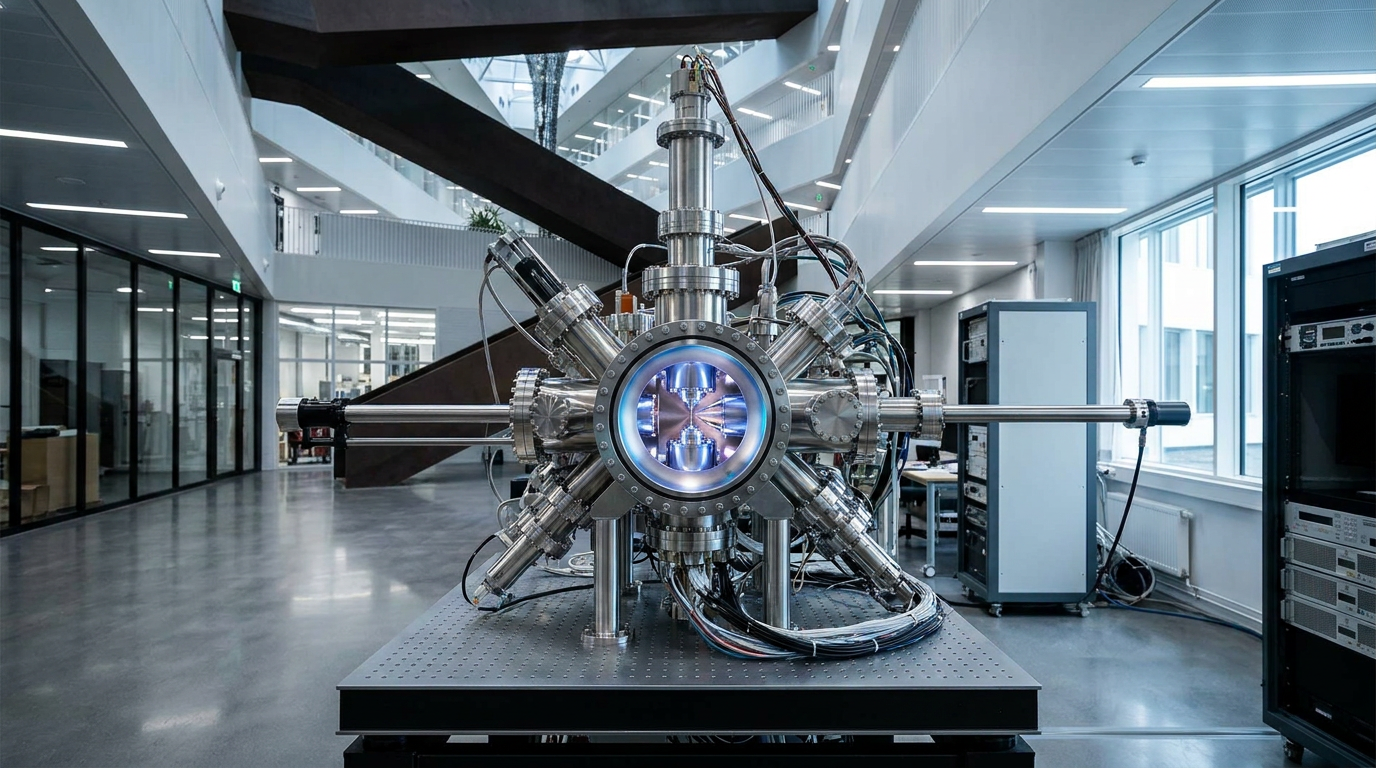
The evidence for the precise synthesis of this 2D topological crystalline insulator is exceptionally strong. The research team built the material by growing exactly two atomic layers of tin telluride on top of a niobium diselenide substrate. They utilized molecular beam epitaxy, a highly precise technique for atomic-layer deposition, to ensure the layers were flawless.[1][2][4]

To verify the structure, the team employed low-temperature scanning tunneling microscopy. This provided direct, atomic-resolution imaging of the lattice and confirmed the physical presence of the conducting edge states running along the boundaries of the tin telluride.[3][5]
A critical secondary claim is that the topological properties do not exist in isolated tin telluride, but are instead forced into existence by the underlying substrate. The scanning tunneling microscopy measurements reveal a lattice mismatch between the tin telluride film and the niobium diselenide base, which subjects the top layer to immense compressive strain.[1][2][6]
First-principles quantum mechanical calculations conducted by the team perfectly match the experimental microscopy data. These models confirm that without this specific, substrate-induced mechanical compression, the topological phase would not open, and the material would behave as a standard insulator.[1][3][4]
Building on this, the researchers assert that engineers can actively tune the material's electronic behavior by adjusting the applied strain—a concept known as "straintronics." By probing the material at the atomic level, the researchers observed exactly how neighboring edge states interact when the lattice is perturbed.[3][7]
The microscopy data showed clear energy shifts driven by electrostatic interactions and quantum tunneling. This proves that the electronic pathways respond dynamically to structural strain, providing strong evidence that the conductivity can be manipulated mechanically.[1][2][4]
The microscopy data showed clear energy shifts driven by electrostatic interactions and quantum tunneling.
The most highly anticipated claim is that the material is viable for room-temperature electronics. A persistent hurdle for quantum materials is their reliance on cryogenic cooling, often near absolute zero, to maintain their delicate quantum states without thermal disruption.[3][8]
The evidence for room-temperature viability rests on the material's measured electronic band gap. The data reveals a band gap exceeding 0.2 electron volts. In solid-state physics, a gap of this magnitude is theoretically sufficient to prevent ambient thermal energy at room temperature from scattering the electrons and destroying the protected edge states.[1][2][3][4]

However, there is transparent uncertainty regarding immediate real-world deployment. While the theoretical math strongly supports room-temperature stability, the direct experimental evidence remains incomplete. The microscopy measurements that confirmed the edge states were performed at cryogenic temperatures to achieve the necessary atomic precision. Direct observation of lossless edge conduction at 300 Kelvin has not yet been published.[1][5]
Furthermore, scaling this technology presents a formidable materials science challenge. Molecular beam epitaxy is a slow, expensive process used for microscopic laboratory samples. Transitioning from a two-layer microscopic flake to commercial-scale wafer manufacturing will require entirely new fabrication techniques.[5][7]
Despite these scaling challenges, the underlying physics represents a paradigm shift. In a topological crystalline insulator, electrons travel along the boundaries without backscattering, effectively eliminating electrical resistance and heat generation.[4][6]
Because these edge states lock the electron's momentum to its quantum spin, the material is an ideal candidate for spintronics. Spintronic devices use magnetic spin rather than electrical charge to process information, promising a massive leap in computational efficiency.[3][4][8]

The ability to manipulate these spintronic pathways simply by flexing or straining the material opens the door to ultra-low-power nanoscale transistors. Instead of relying on continuous electrical currents, future devices could process data through microscopic mechanical adjustments.[7][8]
How we got here
2012
Theoretical physicists first predict the existence of two-dimensional topological crystalline insulators.
2022
Researchers begin experimenting with van der Waals heterostructures to engineer artificial topological states.
Jan 2026
The Finnish research team publishes their initial findings on strain-induced topological states in bilayer tin telluride.
July 2026
The breakthrough gains widespread recognition as a viable platform for room-temperature quantum electronics.
Viewpoints in depth
Quantum Materials Physicists
Focus on the fundamental achievement of realizing a long-predicted topological crystalline insulator.
For theoretical and experimental physicists, the primary triumph is the physical realization of a phase of matter predicted over a decade ago. Topological crystalline insulators differ from standard topological insulators because their conducting states are protected by the spatial symmetry of the crystal lattice itself, rather than time-reversal symmetry. Physicists emphasize that proving this theory required atomic-precision measurements at cryogenic temperatures to definitively map the edge states without thermal noise. Their focus remains on exploring the fundamental quantum tunneling and electrostatic interactions that occur when these edge states are perturbed.
Device Engineers
Emphasize the practical applications of strain-controllable edge states for room-temperature spintronics.
Engineers view this breakthrough through the lens of 'straintronics' and next-generation computing. Traditional silicon transistors are approaching their physical limits, generating unsustainable amounts of heat. Because this new material features a band gap of 0.2 eV, engineers argue it is uniquely positioned to support lossless, room-temperature electron transport. By applying microscopic mechanical strain to the material, future devices could toggle conductivity on and off without the energy loss associated with moving electrical charges, paving the way for ultra-low-power spintronic processors.
Materials Synthesis Experts
Highlight the immense fabrication challenges involved in scaling the material for commercial use.
While acknowledging the breakthrough, materials scientists point out the severe limitations of the current manufacturing process. The material was synthesized using molecular beam epitaxy to deposit exactly two layers of tin telluride onto a niobium diselenide substrate—a painstaking, expensive technique restricted to laboratory environments. Synthesis experts argue that before this quantum material can revolutionize consumer electronics, the industry must develop scalable, high-throughput fabrication methods capable of producing these delicate van der Waals heterostructures on commercial silicon wafers without introducing defects.
What we don't know
- Whether the lossless edge conduction can be definitively observed and maintained at 300 Kelvin outside of cryogenic testing environments.
- How quickly the molecular beam epitaxy synthesis method can be scaled up for commercial wafer manufacturing.
- Which specific spintronic device architectures will best leverage the strain-controllable properties of this new material.
Key terms
- Topological Crystalline Insulator
- A phase of matter that is insulating in its bulk but features conducting states on its surfaces or edges, protected by the crystal's spatial symmetry.
- Molecular Beam Epitaxy
- A highly precise method of depositing single layers of atoms to build ultra-thin crystalline materials.
- Scanning Tunneling Microscopy
- An imaging technique that uses a microscopic probe to visualize and manipulate individual atoms on a material's surface.
- Spintronics
- An emerging technology that uses the intrinsic spin of electrons, rather than their electrical charge, to store and process data.
- Band Gap
- The energy difference between the highest occupied electron state and the lowest unoccupied state, determining a material's electrical conductivity.
Frequently asked
What is a topological crystalline insulator?
It is a phase of matter that acts as an electrical insulator in its interior but conducts electricity perfectly along its edges, protected by the symmetry of its crystal lattice.
Why is the 0.2 eV band gap important?
A band gap of more than 0.2 electron volts is large enough to prevent ambient heat from disrupting the quantum states, making room-temperature operation theoretically possible.
How does strain control the material?
The underlying substrate compresses the tin telluride layers. By adjusting this mechanical strain, engineers can tune the material's electronic properties and conductivity.
What are the practical applications?
This material could enable spintronics and ultra-low-power nanoscale devices that process information without the heat and energy loss of traditional silicon transistors.
Sources
Source coverage
8 outlets
3 viewpoints surfaced








[1]Nature CommunicationsQuantum Materials Physicists
Strain-induced two-dimensional topological crystalline insulator in bilayer SnTe
Read on Nature Communications →[2]University of JyväskyläQuantum Materials Physicists
Researchers realized long-sought two-dimensional topological material
Read on University of Jyväskylä →[3]ScienceDailyDevice Engineers
2d Topological Material Realized
Read on ScienceDaily →[4]SciTechDailyDevice Engineers
Researchers in Finland have experimentally realized a long-predicted class of quantum material
Read on SciTechDaily →[5]Aalto UniversityQuantum Materials Physicists
Control of molecular orbital ordering using a van der Waals monolayer
Read on Aalto University →[6]Positron TodayScience Communicators
Physicists finally build a quantum material predicted more than a decade ago
Read on Positron Today →[7]Physics WorldDevice Engineers
Strain engineering to reveal novel electronic phases
Read on Physics World →[8]The Daily News NowScience Communicators
First Real Quantum Material Made
Read on The Daily News Now →

Every angle. Every day.
Get science stories with full source coverage and perspective breakdowns delivered to your inbox.