Nanoscale Substrate Sculpting Unlocks Higher Temperatures and Magnetic Tolerance in Superconductors
By carving microscopic ridges into the foundation beneath an ultrathin superconducting film, researchers have drastically improved its ability to operate at higher temperatures and withstand intense magnetic fields.
By Factlen Editorial Team
- Materials Scientists
- Views the breakthrough as a paradigm shift from chemical discovery to structural geometry in the pursuit of stronger superconductors.
- Quantum Computing Engineers
- Focuses on the massive 50-Tesla increase in magnetic field tolerance, which is critical for stabilizing fragile quantum bits.
- Energy Infrastructure Analysts
- Highlights the potential for these ultra-efficient materials to drastically reduce the 6 to 12 percent of global electricity consumed by data centers.
What's not represented
- · Semiconductor Manufacturers
- · Commercial Data Center Operators
Why this matters
Modern digital infrastructure consumes up to 12 percent of global electricity, a figure that is rapidly climbing with the AI boom. By proving that the physical shape of a material's foundation can drastically improve its ability to conduct electricity without loss, this breakthrough provides a completely new blueprint for building ultra-efficient power grids and stable quantum computers.
Key points
- Researchers enhanced superconductivity by sculpting the underlying substrate rather than altering the material's chemistry.
- The nanoscale ridges and valleys guide the atoms of the superconducting film, creating a highly stable electronic landscape.
- The modified 10-nanometer film stayed superconducting at temperatures 15 Kelvin higher than standard flat films.
- The sculpted design also allowed the material to tolerate magnetic fields more than 50 Tesla stronger.
- The breakthrough offers a new design principle for developing ultra-efficient electronics and quantum components.
The modern digital world is running into a hard physical limit: heat and resistance. Data centers, information networks, and consumer devices currently consume between 6 and 12 percent of global electricity, much of which is lost as waste heat as electrons push their way through copper wires and silicon chips. For decades, physicists have viewed superconductors—materials that carry electrical current with absolutely zero resistance—as the ultimate solution to this energy drain.[3][6]
However, superconductors come with severe caveats that have kept them largely confined to specialized laboratory environments and MRI machines. To achieve zero resistance, these materials typically must be cooled to extreme temperatures, often hovering near absolute zero. Furthermore, the quantum state that allows electrons to flow freely is notoriously fragile, easily shattered by the presence of strong magnetic fields.[3][4][5]
Over the past thirty years, the primary strategy for overcoming these limitations has been chemical. Materials scientists have relentlessly tweaked the atomic recipes of various compounds, searching for a magic mixture that might remain superconducting at room temperature. While this chemical hunt has yielded progress, particularly with a family of copper-oxide materials known as cuprates, the gains have stubbornly plateaued in recent years.[3][5]
Now, an international team led by researchers at Chalmers University of Technology in Sweden has demonstrated a radical departure from the chemical approach. In a study published in the journal Nature Communications in June 2026, the team proved that the key to stronger superconductivity does not necessarily lie in the material itself, but in the physical geometry of the surface it rests upon.[1][2]

The breakthrough centers on the concept of a substrate—the foundational layer upon which ultrathin films of superconducting materials are grown during fabrication. Traditionally, these substrates are engineered to be as perfectly flat and uniform as possible. The Chalmers team, working alongside the RISE Research Institutes of Sweden, hypothesized that a flat surface might actually be limiting the material's potential.[1][3]
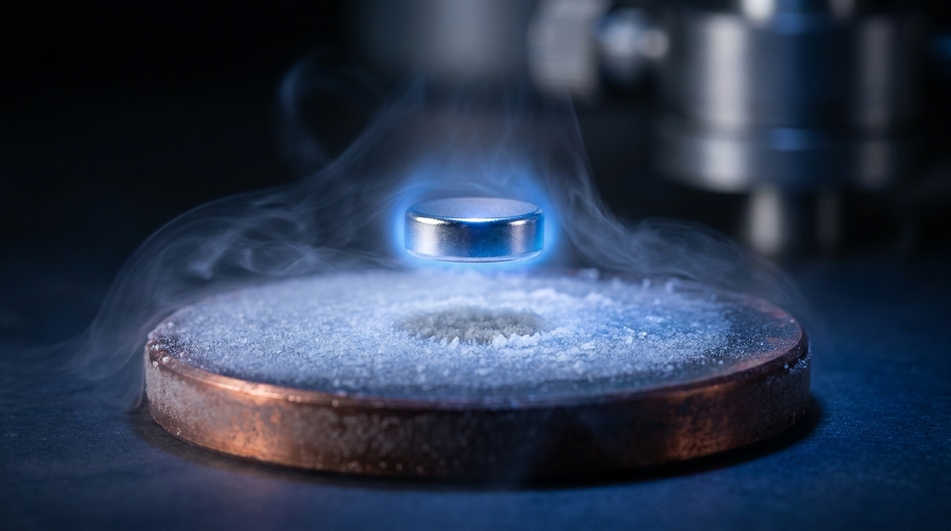
To test this, the researchers focused on a widely studied cuprate superconductor known as YBa₂Cu₃O₇−δ, or YBCO. They grew an ultrathin layer of this material—just 10 nanometers thick, or less than one-millionth the thickness of a human hair—on a magnesium oxide substrate. But before depositing the superconductor, they fundamentally altered the substrate's topography.[3][6][7]
By pre-treating the magnesium oxide in a vacuum at high temperatures, the team induced a thermal reconstruction of the surface. This process sculpted a quasi-periodic landscape of microscopic ridges and valleys, known as nanofacets, across the substrate. Instead of a flat plain, the foundation became a highly textured, corrugated terrain at the nanometer scale.[4][5][6]
When the ultrathin YBCO film was subsequently grown on this textured surface, the results were dramatic. "Because the atoms in the substrate are arranged in a specific pattern, they can 'guide' how the atoms in the superconducting layer settle," explained Eric Wahlberg, a researcher at RISE. The physical shape of the foundation forced the superconducting atoms into a highly specific alignment.[1][3]

This geometric guidance created a distinct electronic environment at the interface between the two materials. The researchers observed that the electronic potential induced by the ridges steered the material's charge-density waves into a single, preferential direction. This nematic behavior—where electrons align themselves in a structured pattern—actively stabilized and strengthened the overall superconducting state.[4][6][7]
This geometric guidance created a distinct electronic environment at the interface between the two materials.
The performance metrics of the sculpted material shattered expectations. Compared to standard 50-nanometer films grown on flat surfaces, the 10-nanometer film on the nanofaceted substrate maintained its superconductivity at an onset temperature more than 15 Kelvin higher, reaching around 90 Kelvin. While still extremely cold, a 15-degree jump achieved purely through structural engineering is considered a massive leap in condensed matter physics.[5][7]
Even more crucially, the sculpted material demonstrated an unprecedented resilience to magnetic interference. The researchers found that the nanofaceted YBCO film could tolerate magnetic fields more than 50 Tesla stronger than its flat-substrate counterparts. To confirm that the geometry was solely responsible for the boost, the team tested an identical 10-nanometer film on a flat magnesium oxide substrate, which showed absolutely no enhancement.[7]
"By sculpting the surface that the superconductor rests on, we were able to induce superconductivity at significantly higher temperatures than previously possible," noted Floriana Lombardi, Professor of Quantum Device Physics at Chalmers and the study's lead author. She emphasized that these very small changes at the nanoscale can have decisive, macroscopic effects on how electricity flows.[2][3][4]
This resilience to magnetic fields solves a major engineering paradox in the development of quantum computers. Quantum bits, or qubits, often rely on superconducting circuits to function without losing their delicate quantum states. However, manipulating these qubits frequently requires the application of localized magnetic fields, which ironically threatens to destroy the very superconductivity the system depends on.[2][4][5]

By providing a buffer of an additional 50 Tesla, the nanofaceted substrate design offers quantum engineers a much wider operational margin. This could allow for the design of more compact, densely packed quantum processors where magnetic cross-talk between adjacent components is less likely to trigger a catastrophic loss of superconductivity.[2][6][7]
Beyond quantum computing, the implications for global energy infrastructure are profound. The ability to engineer stronger superconductivity into ultrathin films opens the door to highly efficient power modules and high-frequency power conversion systems. These components are the critical bottlenecks in electric vehicle drivetrains, renewable energy storage systems, and the massive power supplies required by modern data centers.[3][6]
The true paradigm shift of the Chalmers study is conceptual. It proves that the carrier density and electronic ground state of cuprates—which are notoriously difficult to tune after the material is synthesized—can be manipulated externally through the physical interface. This introduces a new lever for process control that does not require discovering entirely new elements or compounds.[5][6]
"Instead of searching for entirely new materials or manipulating the chemical properties of existing ones, we are now showing how superconductivity can be enhanced by sculpting the substrate," Lombardi stated. This realization effectively opens a new sub-field of topological materials science, where the physical architecture of a component is just as important as its chemical recipe.[1][3][4]

Moving forward, the research community will need to determine if this nanofaceting technique can be generalized. While the results with YBCO and magnesium oxide are definitive, it remains to be seen if similar geometric sculpting can boost the performance of other superconducting families, such as iron-based compounds or the recently discovered nickelates.[2][6]
There are also practical hurdles regarding industrial scalability. Pre-treating substrates in high-temperature vacuums is a standard procedure in advanced semiconductor fabrication, but maintaining the precise quasi-periodic landscape of the nanofacets across large-scale wafers will require rigorous quality control. The transition from a controlled laboratory demonstration to commercial foundries will likely take years of iterative engineering.[3][4][6]
Nevertheless, the demonstration that geometry can conquer the magnetic and thermal fragility of superconductors marks a definitive turning point. By looking beneath the material itself and reshaping its foundation, physicists have unlocked a new blueprint for the ultra-efficient, zero-loss electrical systems that the next generation of digital infrastructure will desperately need.[3][5]
How we got here
1986
The discovery of high-temperature cuprate superconductors sparks hopes for lossless energy transmission.
2010s
Progress in raising superconducting temperatures stalls as chemical manipulation of cuprates hits a plateau.
2017
The Chalmers University team begins experimenting with nanoscale substrate modifications to influence electron behavior.
Early 2026
Researchers successfully test a 10-nanometer YBCO film on a nanofaceted magnesium oxide substrate, recording unprecedented stability.
June 17, 2026
The breakthrough is published in Nature Communications, detailing the +15 K temperature boost and +50 Tesla magnetic tolerance.
Viewpoints in depth
Materials Scientists' view
Focuses on the shift from chemical discovery to geometric engineering.
For decades, the field of superconductivity has chased new compounds and chemical mixtures in the hopes of finding a room-temperature superconductor. This breakthrough proves that manipulating the physical interface of existing cuprates can yield massive performance gains. By demonstrating that the substrate's topography can actively steer charge-density waves, researchers have opened a new sub-field of topological substrate engineering, where physical architecture is just as vital as chemical composition.
Quantum Computing Engineers' view
Emphasizes the critical importance of the 50-Tesla increase in magnetic field tolerance.
Quantum states are notoriously fragile, and the magnetic fields required to operate qubits often destroy the superconductivity of the surrounding components. An extra 50 Tesla of magnetic tolerance is a game-changer for qubit stability. It provides engineers with a much wider operational margin, allowing for the design of more compact, densely packed quantum processors where magnetic cross-talk is less likely to trigger a catastrophic system failure.
Energy Infrastructure Analysts' view
Highlights the potential to drastically reduce the massive energy drain of modern data centers.
With AI and data centers pushing global ICT electricity consumption toward 12 percent, highly stable superconductors are the holy grail for lossless power transmission and ultra-efficient server farms. While this specific breakthrough still requires extreme cold, the geometric design principle provides a viable new pathway toward near-room-temperature superconductors, which would fundamentally transform the economics of the global energy grid.
What we don't know
- Whether this nanofaceted substrate technique can be successfully applied to other classes of superconductors beyond cuprates.
- How easily the high-temperature vacuum pre-treatment process can be scaled for mass industrial manufacturing.
- The theoretical upper limit of temperature gains achievable purely through geometric substrate sculpting.
Key terms
- Superconductor
- A material that can conduct electricity with zero resistance and zero energy loss when cooled below a certain critical temperature.
- Cuprate
- A class of copper-oxide materials known for exhibiting superconductivity at relatively high temperatures compared to conventional metals.
- Substrate
- The underlying foundation or template upon which ultrathin films of materials are grown during fabrication.
- Nanofacets
- Microscopic ridges and valleys sculpted into a surface at the nanometer scale, used to guide atomic arrangement.
- Charge-density wave
- A quantum mechanical phenomenon where electrons form a standing wave pattern, which can compete with or enhance superconductivity.
- Onset temperature
- The specific temperature at which a material begins to transition into a superconducting state.
Frequently asked
What is the main breakthrough in this study?
Researchers found that sculpting microscopic ridges into the surface beneath a superconductor, rather than changing its chemistry, makes it function at higher temperatures and withstand stronger magnetic fields.
Why do magnetic fields matter for superconductors?
Strong magnetic fields typically destroy the superconducting state. This is a major hurdle because many applications, like quantum computers and MRI machines, rely on powerful magnets to operate.
Does this mean we have room-temperature superconductors?
Not yet. The onset temperature was raised by 15 Kelvin (to around 90 K), which is still extremely cold, but the geometric design principle provides a completely new path toward that ultimate goal.
How much energy could this technology save?
Digital devices and data centers currently consume 6 to 12 percent of global electricity. Widespread use of lossless superconductors could drastically reduce this massive energy drain.
Sources
Source coverage
7 outlets
3 viewpoints surfaced


[1]Nature CommunicationsMaterials Scientists
Boosting superconductivity in ultrathin YBa₂Cu₃O₇−δ films via nanofaceted substrates
Read on Nature Communications →[2]Chalmers University of TechnologyMaterials Scientists
Superconductivity breakthrough could unlock ultra-efficient electronics
Read on Chalmers University of Technology →[3]ScienceDailyEnergy Infrastructure Analysts
A clever nanoscale redesign may have solved one of superconductivity's biggest problems
Read on ScienceDaily →[4]SciTechDailyQuantum Computing Engineers
Robust superconductivity via new approach
Read on SciTechDaily →[5]EurekAlertEnergy Infrastructure Analysts
A new design principle for future superconductors
Read on EurekAlert →[6]SuperVeniceEnergy Infrastructure Analysts
Superconductivity gets a Boost from Nanoscale Substrate Design
Read on SuperVenice →[7]JerryCards ScienceQuantum Computing Engineers
Physicists Sculpted a Surface at the Nanoscale - and Made a Superconductor Run Hotter
Read on JerryCards Science →
Every angle. Every day.
Get science stories with full source coverage and perspective breakdowns delivered to your inbox.