How Photonic Chips Are Using Light to Break the AI Energy Bottleneck
As artificial intelligence pushes traditional silicon to its physical limits, a new generation of hardware is replacing electricity with light to process data at unprecedented speeds.
By Factlen Editorial Team
- Photonic Hardware Developers
- Argue that optical interconnects and compute are the only viable way to break the AI memory wall and scale sustainably.
- Traditional Silicon Incumbents
- View photonics primarily as a complementary interconnect technology rather than a full replacement for electronic GPU compute cores.
- Materials Scientists
- Focus on solving the fundamental physics bottlenecks, like nonlinear all-optical switching, to make fully optical chips a reality.
What's not represented
- · Data center cooling operators
- · Quantum computing researchers
Why this matters
As artificial intelligence models grow exponentially, they are pushing the global power grid to its limits. Photonic computing offers a physical escape route from this energy crisis, promising to make AI faster, vastly more energy-efficient, and sustainable for the next decade of technological progress.
Key points
- AI data centers are hitting a "memory wall," where moving data over copper wires consumes more energy than computing it.
- Photonic chips replace electricity with light, using microscopic waveguides to process data with near-zero resistance.
- Optical neural networks perform complex matrix math passively as light passes through interference units.
- Major investments, including Marvell's $3.25 billion acquisition of Celestial AI, signal the commercial arrival of optical interconnects.
- Researchers are overcoming final hurdles, such as all-optical switching, to pave the way for fully light-based AI processors.
The artificial intelligence boom has collided with a physical wall. As technology giants race to build data centers capable of training trillion-parameter models, the infrastructure is buckling under the constraints of copper and electricity. Modern AI clusters require hundreds of miles of heavy copper cabling just to link processors together, generating immense heat and drawing gigawatts of power.[3][8]
The core bottleneck is no longer the speed of the processors themselves, but the energy required to feed them. Engineers call this the "memory wall." In a modern AI system, a staggering amount of energy is spent not on actual calculation, but simply shuttling data back and forth between memory banks and compute cores. As electrical signals travel across copper wires, they encounter resistance, degrading the signal and bleeding energy as heat.[1][2][3]
To break this bottleneck, the semiconductor industry is turning to a radically different medium: light. Photonic AI chips, which use photons instead of electrons to transmit and process data, are moving rapidly from experimental physics labs into commercial data centers. By harnessing the unique properties of light, these optical neural networks promise to execute the massive mathematical workloads of AI at unprecedented speeds while consuming a fraction of the power.[4][6][8]
The fundamental advantage of photonic computing lies in basic physics. Electrons have mass and carry an electrical charge; when forced through a copper wire or a silicon transistor, they bump into each other and the surrounding material, creating friction and heat. Photons, the fundamental particles of light, have no mass and no charge. They can glide through optical pathways without resistance, allowing data to move with near-zero energy loss.[6][8]

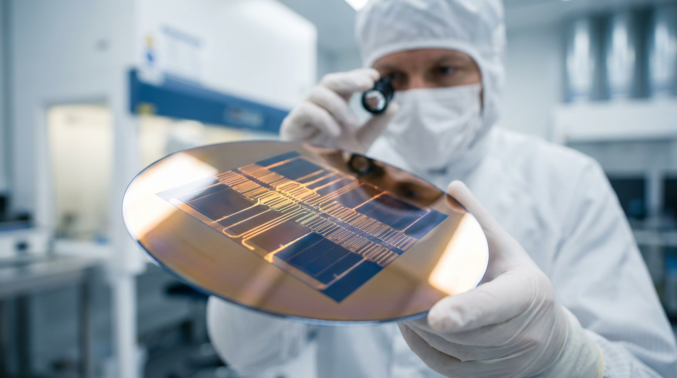
Building a computer out of light requires a manufacturing technique known as silicon photonics. Rather than discarding decades of semiconductor infrastructure, engineers use standard fabrication facilities to etch microscopic channels, called waveguides, directly into silicon wafers. These waveguides act as optical highways, steering beams of light around the chip just as copper traces steer electrical currents.[4][6][8]
A functional photonic chip relies on a specific sequence of components. It begins with a laser that generates a continuous, stable beam of light. Because a steady beam carries no information, the light passes through a modulator, which rapidly alters the wave's amplitude or phase to encode digital data. Once the data is encoded, the light is sent through the waveguide network to be processed.[4][6][8]
The true breakthrough of optical neural networks is how they perform mathematical calculations. The backbone of any AI model is matrix multiplication—a process of multiplying massive grids of numbers together. In a traditional electronic graphics processing unit (GPU), these calculations are performed sequentially, requiring the chip to constantly open and close billions of microscopic transistor gates.[6][8]
Photonic chips perform this math passively. Using a technique known as parallel optical matrix-matrix multiplication, the encoded light waves are directed through a series of optical interference units. As the light beams cross paths and interfere with one another, the physical blending of the waves naturally computes the mathematical result. The calculation happens instantly as the light passes through, achieving what researchers call "physics-level parallelism."[6][7][8]

Using a technique known as parallel optical matrix-matrix multiplication, the encoded light waves are directed through a series of optical interference units.
Because the math is performed by the natural interference of light rather than the switching of electrical gates, the energy savings are profound. In a photonic integrated circuit, the phase modulators that control the light draw as little as 10 milliwatts of power—orders of magnitude less than the kilowatt-scale power draw of electronic GPU clusters running equivalent workloads.[6]
While fully optical compute processors are still maturing, the first massive commercial application for photonics is in chip-to-chip communication, known as optical interconnects. Companies are replacing the copper wires that link GPUs together with fiber optics integrated directly into the chip packaging, solving the data movement crisis at the hardware level.[1][2][4]
Lightmatter, a Boston-based startup that recently raised $850 million, has developed an interconnect platform called Passage. The technology uses "edgeless I/O" to route data optically across the entire surface of a chip, rather than just at the edges. By utilizing bidirectional communication—sending and receiving light on the same fiber—Lightmatter aims to cut the estimated 300 miles of cabling required in next-generation AI clusters by half.[1][3]
The scale of the interconnect market was underscored in late 2025 when semiconductor giant Marvell acquired Celestial AI for $3.25 billion. Celestial AI's "Photonic Fabric" technology delivers 16 terabits per second of bandwidth in a single chiplet, allowing massive AI clusters to share memory and compute resources seamlessly over optical links.[2][4]

Despite these massive investments, fully optical AI computation faces a stubborn physical hurdle known as the "translation tax." While light is perfect for the linear matrix math of AI, neural networks also require nonlinear "activation functions"—the decision rules that determine whether a neuron should fire and pass information to the next layer.[5][7][8]
Traditionally, photonic chips have had to convert the light signal back into electricity to perform these nonlinear decisions, eroding the speed and efficiency gains of the optical system. However, researchers are making rapid progress on all-optical logic. In early 2026, physicists at the University of Pennsylvania demonstrated ultra-low-energy optical switching using exciton-polaritons—hybrid quasiparticles that combine light and matter, allowing photons to interact strongly enough to compute decisions without electrical conversion.[5]
Manufacturing also presents unique challenges. Silicon, the bedrock of the semiconductor industry, is excellent at guiding light but physically incapable of generating it. To solve this, manufacturers must use hybrid integration, carefully bonding lasers made from exotic III-V materials, like indium phosphide, onto the silicon wafers.[4][8]
Furthermore, photonic components are fundamentally constrained by the wavelength of light itself. While electronic transistors have shrunk to the size of a few nanometers, optical waveguides and modulators must remain relatively large to properly contain the light waves. This limits the packing density of photonic chips, meaning they cannot simply replicate the billions of components found on modern electronic processors.[8]

Because of these physical constraints, the immediate future of AI hardware is not a wholesale replacement of silicon, but a hybrid approach. Co-packaged optics will see photonic chiplets sitting side-by-side with traditional electronic GPUs, handling the massive data movement and specific linear calculations while the electronic cores manage the complex logic.[1][3][8]
As the demands of artificial intelligence continue to outpace the physical limits of traditional electronics, the transition to light-based computing is no longer a theoretical luxury, but an infrastructural necessity. By replacing the friction of electrons with the frictionless glide of photons, the semiconductor industry is laying the groundwork for a more powerful, and vastly more sustainable, era of computing.[2][4][8]
How we got here
2016
Foundational patents are filed for using optical interference units in neural networks.
2020–2023
Startups like Lightmatter and Celestial AI demonstrate viable silicon photonics prototypes.
Dec 2025
Marvell acquires Celestial AI for $3.25 billion, signaling mainstream semiconductor adoption.
Early 2026
Lightmatter joins Nvidia's NVLink Fusion ecosystem to integrate optics with dominant GPUs.
April 2026
UPenn researchers demonstrate ultra-low-energy all-optical switching using hybrid particles.
Viewpoints in depth
Photonic Hardware Developers
Startups and optical engineers argue that light is the only scalable path forward for AI.
Companies like Lightmatter and Celestial AI view the current reliance on copper interconnects as a dead end. They argue that as AI models scale into the trillions of parameters, the energy required simply to move data between GPUs will outstrip the power available to data centers. By integrating photonics directly into the chip packaging, they believe the industry can decouple computational growth from energy consumption, enabling the next generation of frontier AI models without melting the power grid.
Traditional Silicon Incumbents
Major chipmakers view photonics as a vital complement to, rather than a replacement for, electronic GPUs.
While legacy semiconductor giants are investing heavily in photonics—evidenced by Marvell's multi-billion-dollar acquisitions and Nvidia's partnerships—they generally view light as an interconnect solution rather than a compute replacement. Because optical components cannot be miniaturized to the nanometer scale of electronic transistors, incumbents argue that the future is "co-packaged optics." In this view, silicon GPUs will continue to handle the complex logic and computation, while photonic chiplets act as ultra-fast, low-power highways connecting the electronic brains together.
Materials Scientists
Academic researchers are focused on solving the fundamental physics bottlenecks that prevent fully optical computing.
Physicists and materials scientists point out that current commercial photonic chips still rely on a "translation tax"—converting light back to electricity to perform nonlinear decision-making. Researchers at institutions like the University of Pennsylvania are working at the quantum level to create hybrid light-matter particles that allow photons to interact directly. They argue that until these fundamental physics challenges are solved and all-optical logic is perfected, photonic chips will remain specialized accelerators rather than universal processors.
What we don't know
- How quickly the semiconductor supply chain can scale the mass production of hybrid indium-phosphide and silicon chips.
- Whether fully optical processors will ever achieve the packing density required to completely replace electronic GPU cores.
- How the software ecosystem will adapt to compile traditional AI models seamlessly onto optical hardware.
Key terms
- Silicon Photonics
- The practice of building optical components, like waveguides and modulators, directly onto traditional silicon wafers.
- Waveguide
- A microscopic channel etched into a chip that steers and confines light, acting like a wire for photons.
- Optical Interconnect
- A system that uses light to transmit data between different chips or servers, replacing traditional copper cables.
- Phase Modulator
- A component that encodes digital data by altering the phase of a light wave as it passes through the chip.
- Exciton-Polariton
- A hybrid quasiparticle combining light and matter, used experimentally to allow photons to interact with each other for optical logic.
Frequently asked
Will photonic chips replace my computer's CPU?
Not anytime soon. Photonic chips are highly specialized for the massive matrix math required by AI and for moving data in data centers, rather than general-purpose computing.
Why can't we just use regular fiber optic cables?
We do use fiber optics for long-distance internet, but inside an AI data center, converting light back to electricity at every chip creates a massive bottleneck. Photonic chips process the light directly.
Are these chips available now?
Yes, early versions focused on chip-to-chip communication (optical interconnects) are currently being deployed in major AI data centers, with fully optical compute processors expected later this decade.
Sources
Source coverage
8 outlets
3 viewpoints surfaced


[1]LightmatterPhotonic Hardware Developers
A New Computing Pathway: Photonic AI Processing
Read on Lightmatter →[2]MarvellPhotonic Hardware Developers
Celestial AI and Photonic Fabric
Read on Marvell →[3]Business InsiderTraditional Silicon Incumbents
Inside Lightmatter's photonics hardware for AI data centers
Read on Business Insider →[4]IDTechEx
Silicon Photonics and Photonic Integrated Circuits 2026-2036
Read on IDTechEx →[5]University of PennsylvaniaMaterials Scientists
Penn physicists create hybrid light-matter particles for optical AI
Read on University of Pennsylvania →[6]PatSnap InsightsMaterials Scientists
Optical neural networks: replacing electrons with photons
Read on PatSnap Insights →[7]SPIEMaterials Scientists
Photonic multisynapse neural networks for AI computation
Read on SPIE →[8]Factlen Editorial Team
Synthesis by Factlen editorial team
Read on Factlen Editorial Team →


Every angle. Every day.
Get ai stories with full source coverage and perspective breakdowns delivered to your inbox.