How Photonic Chips Are Using Light to Solve AI's Massive Energy Crisis
As traditional electronic GPUs hit their physical limits, a new generation of photonic processors is using lasers and optical pathways to perform AI calculations at the speed of light.
By Factlen Editorial Team
- Hardware Innovators
- Researchers and startups pushing for a fundamental shift away from electronic computing to sustain AI growth.
- Geopolitical Strategists
- Nations viewing photonics as a way to rewrite the rules of the semiconductor supply chain and bypass export controls.
- Incumbent Chipmakers
- Traditional semiconductor giants integrating light into existing silicon ecosystems primarily for data transfer.
What's not represented
- · Environmental groups monitoring data center emissions
- · Cloud computing infrastructure operators
Why this matters
Artificial intelligence is currently constrained by the massive electricity demands and heat generation of traditional silicon chips. By computing with light instead of electricity, photonics could shatter this bottleneck, enabling vastly more powerful AI models while preventing the technology from overwhelming global power grids.
Key points
- Traditional electronic GPUs are hitting physical limits, generating massive heat and consuming vast amounts of electricity to train AI models.
- Photonic AI chips solve this by using lasers and microscopic optical pathways to perform complex matrix multiplication at the speed of light.
- Because photons travel without electrical resistance, optical processors can achieve up to 100 times the energy efficiency of traditional silicon.
- Recent breakthroughs in hybrid light-matter particles have allowed optical chips to perform complex nonlinear decision-making steps.
- Nations like China and the UK are heavily investing in photonics as a strategic pathway to bypass traditional semiconductor supply chain bottlenecks.
The artificial intelligence boom has collided with a fundamental law of physics: pushing electrons through copper wires generates heat. For decades, the semiconductor industry has sustained progress by shrinking transistors, packing billions of them onto a single piece of silicon. But as these components approach the size of a few atoms, the physical limits of electronic computing are becoming impossible to ignore. The resistance encountered by electrical currents creates massive thermal output, requiring data centers to deploy elaborate, energy-intensive liquid cooling systems just to keep the hardware from melting.[1][9]
As AI models scale into the trillions of parameters, the infrastructure required to train and run them is drawing enough electricity to power small cities. Industry analysts and government officials are increasingly warning that this trajectory is unsustainable. If the energy demands of artificial intelligence continue to double at their current rate, the technology threatens to overwhelm regional power grids and derail international clean energy targets. The solution to this crisis, researchers argue, is not to build a slightly better electronic transistor, but to abandon the electron entirely.[8][9]
A radical paradigm shift is now moving from university laboratories to commercial semiconductor foundries. Instead of relying on electrical currents, a new generation of hardware—known as photonic AI chips—uses particles of light to perform computations. By replacing copper wires with microscopic optical pathways and lasers, these processors promise to perform the heavy mathematical lifting of artificial intelligence at the speed of light, while consuming only a fraction of the energy required by traditional silicon. This is not merely a theoretical concept; working prototypes are already demonstrating performance that rivals the most advanced electronic hardware on the market.[1][2]
To understand why photonics is uniquely suited for this moment, one must look at how modern artificial intelligence actually works under the hood. Deep learning neural networks do not process information in the sequential, step-by-step manner of a traditional computer program. Instead, they rely on massive blocks of matrix multiplication—essentially, adding and multiplying millions of numbers simultaneously to recognize patterns in data, whether that data represents pixels in an image or words in a sentence. This specific type of highly parallel, dense mathematics is exactly where optical computing shines brightest, offering a level of intrinsic parallelism that electronics cannot match.[1][7]

In a traditional Graphics Processing Unit (GPU), a shocking amount of power is wasted on logistics. Up to 80 percent of a chip's energy is spent not on the actual mathematical calculations, but on shuffling data back and forth between the processor cores and the memory banks. Every time a piece of data moves, it encounters electrical resistance, burning energy and generating heat. This "data movement bottleneck" is the primary reason why scaling up AI clusters has become so extraordinarily expensive and power-hungry.[5][7]
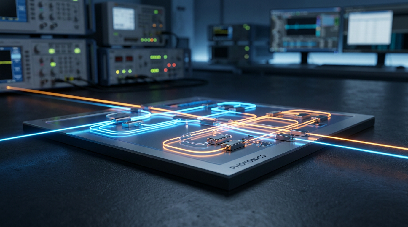
Photonic computing elegantly bypasses this bottleneck. In a photonic integrated circuit, numerical data is encoded directly into the physical properties of light—specifically its amplitude, phase, and wavelength. Because photons have no mass and carry no electrical charge, they do not bump into each other or experience resistance the way electrons do. They can travel through microscopic glass channels, known as waveguides, with virtually zero friction, meaning they generate almost no heat as they move across the chip.[1][6]
The actual computation happens passively. As these encoded light waves pass through specially designed microscopic lenses and interference patterns etched into the silicon, the waves naturally overlap and combine. This physical interference instantly performs the exact matrix multiplications required by the AI model. Where an electronic GPU must use thousands of logic gates flipping on and off to calculate a sum, a photonic chip simply lets the light shine through a lens, completing thousands of calculations simultaneously in a single, continuous flow.[2][6]
This physical interference instantly performs the exact matrix multiplications required by the AI model.
Recent breakthroughs have dramatically accelerated the timeline for this technology. In late 2025, engineers at the University of Florida demonstrated a lens-based photonic chip designed specifically for convolution—the core mathematical task required for image and video recognition. By utilizing microscopic Fresnel lenses to process multiple wavelengths of laser light in parallel, the prototype successfully classified data with 98 percent accuracy. More importantly, it achieved this with up to 100 times the energy efficiency of conventional electronic chips performing the identical task.[6]
Another major hurdle in optical computing has been the "nonlinear" steps in AI processing. While light is perfect for multiplying matrices, neural networks also require decision-making activation functions that are notoriously difficult to perform optically. Historically, systems had to convert the light back into electricity to make these decisions, slowing down the process. However, in May 2026, researchers at the University of Pennsylvania engineered a hybrid light-matter particle called an exciton-polariton, which allows the chip to perform these complex nonlinear steps without ever leaving the optical domain.[4]

The commercial sector is already racing to scale these laboratory innovations into data center infrastructure. Startups like Lightmatter and Celestial AI have raised hundreds of millions of dollars to bring photonic hardware to hyperscale cloud providers. Lightmatter’s "Passage" technology, for instance, uses a photonic interposer to connect thousands of electronic GPUs with optical links. This hybrid approach achieves a staggering 114 terabits per second of bandwidth, drastically cutting the power consumed by data transfer while allowing massive AI clusters to operate as a single unified brain.[5][7]
Crucially, these new optical chips do not require the creation of an entirely new manufacturing ecosystem from scratch. Silicon photonics can be fabricated using the exact same standard CMOS foundry processes that currently produce traditional electronic computer chips. By etching optical waveguides into silicon wafers alongside standard components, engineers can leverage decades of existing semiconductor manufacturing expertise. Major global foundries are already dedicating production lines to optical components, signaling that the technology is rapidly transitioning from bespoke academic prototypes to mass commercial scalability.[2][5]
The implications of this technological shift extend far beyond data center economics; they are actively reshaping global geopolitics and national security strategies. In June 2026, China officially launched a state-backed integrated photonic computing laboratory in Shanghai, bringing together top academic researchers and leading optical startups. This massive industrial partnership is explicitly designed to bypass U.S. export controls, which have severely restricted China's access to the most advanced electronic GPUs required for training frontier artificial intelligence models. By pivoting to light, Beijing hopes to rewrite the rules of the hardware race.[3]
Because photonic chips rely on entirely different physical architectures, they do not strictly require the extreme miniaturization—and the highly restricted extreme ultraviolet (EUV) lithography machines—that define the cutting edge of traditional silicon. A photonic chip manufactured on an older, larger process node can still vastly outperform a state-of-the-art electronic GPU in specific AI tasks simply because light moves faster and cooler than electricity. This offers a parallel pathway to AI supremacy that circumvents existing supply chain choke points.[1][3]

Western governments are acutely aware of this strategic pivot and are mobilizing their own resources to ensure they do not fall behind in the optical computing race. The UK Government’s recently published AI Hardware Plan heavily emphasizes photonic interconnects and optical computing as critical pillars for the nation's future technological sovereignty. Policymakers across Europe and North America increasingly recognize that whoever controls the foundational hardware of the next decade will dictate the pace of global artificial intelligence development, making photonics a matter of urgent national security and economic interest.[8]
True general-purpose optical computers—machines that use light for every single computing task, from running an operating system to rendering a video game—remain years away from commercial viability. The immediate future of artificial intelligence hardware will be deeply hybrid. Electronic GPUs will continue to handle the complex, sequential logic operations and programmable tasks they excel at, while photonic co-processors and optical interconnects will be seamlessly integrated into the same server racks to handle the heavy, parallel mathematics and the massive data transfer requirements of modern neural networks.[1][5]
But the long-term trajectory of the semiconductor industry is now unmistakably clear. The era of relying solely on silicon and electrons to drive the digital revolution is reaching its hard physical limits, constrained by heat, resistance, and the atomic boundaries of matter. As artificial intelligence continues its relentless expansion into every sector of the global economy, the next great leap in computational power will not be achieved by fighting the laws of physics with increasingly elaborate cooling systems. Instead, the future of intelligence will be powered by harnessing the unparalleled speed, bandwidth, and efficiency of light itself.[1][7]
How we got here
1940s
The ENIAC computer establishes the paradigm of using electrons to perform general-purpose calculations.
Dec 2024
MIT researchers demonstrate a fully integrated photonic processor capable of running a neural network optically.
Sep 2025
The University of Florida unveils a light-based chip that performs AI convolution tasks with 100 times the energy efficiency of traditional hardware.
May 2026
University of Pennsylvania scientists create a hybrid light-matter particle to solve the nonlinear computing bottleneck in optical chips.
Jun 2026
China launches a state-backed integrated photonic computing laboratory in Shanghai to bypass U.S. semiconductor export controls.
Viewpoints in depth
The Hardware Innovators
Researchers and startups pushing for a fundamental shift away from electronic computing.
This camp argues that the semiconductor industry is hitting a hard physical wall. As transistors shrink to the size of a few atoms, quantum tunneling and heat dissipation make further efficiency gains nearly impossible. Innovators at institutions like MIT and startups like Lightmatter believe that only a radical shift to optical computing—where data moves and computes as light—can sustain the exponential growth required by next-generation AI models.
Geopolitical Strategists
Nations viewing photonics as a way to rewrite the rules of the semiconductor supply chain.
For countries facing export controls or seeking technological sovereignty, photonics represents a clean slate. Because optical chips rely on different physical architectures, they do not necessarily require the ultra-advanced extreme ultraviolet (EUV) lithography machines monopolized by a few Western companies. China's aggressive investment in optical AI labs is explicitly designed to bypass U.S. restrictions on electronic GPUs, while the UK and Europe view the technology as a chance to reclaim market share in the AI hardware race.
Incumbent Chipmakers
Traditional semiconductor giants integrating light into existing silicon ecosystems.
Established players like Nvidia and TSMC are not ignoring light, but they view it through a different lens. Rather than building pure optical processors, they are focused on 'co-packaged optics'—using photonics strictly to move data between traditional electronic GPUs at high speeds. This camp argues that the flexibility and programmability of electronic transistors cannot be easily replicated by light, making hybrid systems the most realistic path forward for the next decade.
What we don't know
- How quickly the global semiconductor supply chain can pivot its massive electronic foundries to produce optical components at hyperscale volume.
- Whether pure optical processors will eventually replace electronic CPUs entirely, or if the future will remain permanently hybrid.
- How software ecosystems and AI frameworks will need to be rewritten to natively compile code for light-based hardware.
Key terms
- Silicon Photonics
- The integration of optical components, like lasers and waveguides, directly onto standard silicon computer chips.
- Matrix Multiplication
- The core mathematical operation behind artificial intelligence, involving the simultaneous addition and multiplication of massive grids of numbers.
- Waveguide
- A microscopic physical channel etched into a chip that steers and directs particles of light, similar to how a copper wire guides electricity.
- Exciton-Polariton
- A hybrid particle that is half-light and half-matter, allowing optical computers to perform complex decision-making steps without converting signals back to electricity.
Frequently asked
Will photonic chips replace the CPU in my laptop?
No. Photonic chips are highly specialized for the specific types of massive, parallel math required by AI. Your laptop will continue to use traditional electronic processors for everyday tasks.
Why are optical chips more energy efficient?
Unlike electrons, photons (particles of light) have no mass and carry no electrical charge. They travel through optical pathways without resistance, meaning they generate virtually no heat and waste very little energy.
When will this technology be available?
Hybrid systems—where light is used to transfer data between traditional electronic chips—are already entering commercial production. Fully optical AI processors are expected to reach broader data center deployment between 2026 and 2028.
Sources
Source coverage
9 outlets
3 viewpoints surfaced


[1]Factlen Editorial TeamHardware Innovators
Synthesis by Factlen editorial team
Read on Factlen Editorial Team →[2]Massachusetts Institute of TechnologyHardware Innovators
Photonic processor could enable ultrafast AI computations with extreme energy efficiency
Read on Massachusetts Institute of Technology →[3]South China Morning PostGeopolitical Strategists
Facing US chip curbs, China launches photonics lab to power AI with light
Read on South China Morning Post →[4]ScienceDailyHardware Innovators
Forget electrons, this breakthrough uses light-matter particles to power AI
Read on ScienceDaily →[5]EE TimesIncumbent Chipmakers
Photonics Chipmakers Race to Production
Read on EE Times →[6]University of FloridaHardware Innovators
New light-based chip boosts power efficiency of AI tasks 100 fold
Read on University of Florida →[7]LightmatterHardware Innovators
Photonic AI Acceleration - A New Kind of Computer
Read on Lightmatter →[8]UK GovernmentGeopolitical Strategists
UK AI Hardware Plan
Read on UK Government →[9]Microelectronics UKIncumbent Chipmakers
Photonics powering AI data centres: The latest innovations
Read on Microelectronics UK →


Every angle. Every day.
Get ai stories with full source coverage and perspective breakdowns delivered to your inbox.