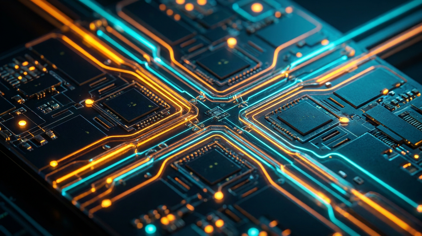
Beyond Silicon: How Photonic Accelerators Are Using Light to Solve AI's Power Crisis
As artificial intelligence models grow exponentially, their energy and data-transfer demands are hitting the physical limits of traditional silicon chips. A new generation of photonic processors is replacing electrons with light, promising to cut AI power consumption by up to 90% while drastically increasing computational speed.
By Factlen Editorial Team
- Photonic Hardware Pioneers
- Argue that light-based computing is the only viable path to scale AI without breaking the global power grid.
- Incumbent Silicon Ecosystem
- Focus on optimizing existing electronic architectures and view photonics primarily as a complementary data-transfer tool rather than a full compute replacement.
- Sustainability Advocates
- Emphasize the critical need to cap the exponential energy growth of AI data centers to meet global carbon targets.
What's not represented
- · Hyperscale Cloud Providers (AWS, Azure, Google Cloud) who must balance the cost of ripping out legacy copper infrastructure against the long-term energy savings of photonics.
- · Grid Operators managing the immediate local power constraints of massive AI data centers.
Why this matters
As artificial intelligence models grow exponentially, their energy demands threaten to overwhelm global power grids and stall future breakthroughs. Photonic computing offers a sustainable path forward, ensuring that the next leap in AI capabilities doesn't come at an unsustainable environmental cost.
Key points
- AI data centers are hitting physical limits, as moving electrons through copper wires generates massive heat and limits data speed.
- Photonic hardware uses lasers instead of electricity to transmit data and perform calculations at the speed of light.
- Recent breakthroughs have achieved a 1.6 Tbps throughput per fiber, an 8X increase over existing optical solutions.
- Optical computing can reduce the power draw of AI inference workloads by 5 to 10 times.
- The technology is moving from the lab to commercial deployment, with co-packaged optics rolling out to hyperscalers in 2025 and 2026.
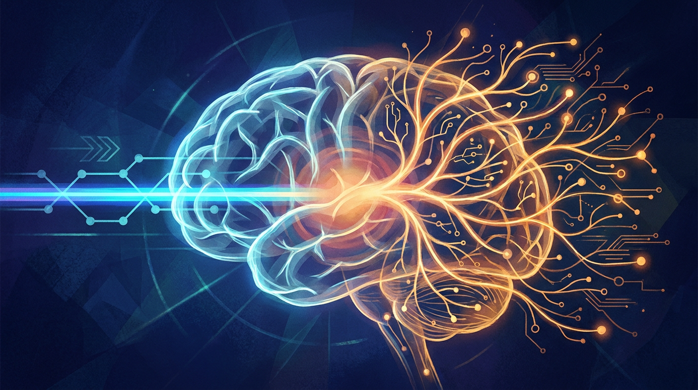
The artificial intelligence revolution has a physics problem. As large language models grow from billions to trillions of parameters, the massive data centers required to train and run them are colliding with the fundamental limits of electricity. The sheer volume of computation is pushing traditional silicon architecture to its absolute breaking point.[3][5]
Inside modern AI clusters, hundreds of thousands of graphics processing units (GPUs) must constantly talk to one another. They do this by pushing electrons through copper wires. But moving electrons generates immense heat, encounters physical resistance, and requires massive amounts of power just to push the signal from one chip to the next.[2][5]
The industry calls this the "interconnect wall." Today, high-performance AI chips are so fast that they spend the majority of their time simply waiting for data to arrive from other chips. The bottleneck is no longer the processor itself, but the physical cables and traces connecting them.[2][3]
To solve this bottleneck, a new generation of hardware disruptors is turning to a completely different medium: light. Photonic AI accelerators and optical interconnects replace traditional electrical signals with lasers, promising to fundamentally rewrite the power and speed equations of artificial intelligence.[2][4]

The concept of optical computing is not entirely new, but it has historically struggled to move from laboratory proof-of-concept to commercial viability. That threshold is now being crossed, driven by the desperate need for efficiency in the generative AI era.[1][7]
In recent months, the field has seen a flurry of breakthroughs. Companies like Lightmatter, which recently reached a $4.4 billion valuation, are demonstrating silicon-proven technologies that integrate directly into existing data center architectures, proving that photonics can scale outside the lab.[2][3]
The core advantage of photonics lies in how light behaves. Unlike electrons, photons do not interfere with one another when their paths cross. This allows engineers to multiplex multiple wavelengths of light—essentially different colors—through a single microscopic waveguide simultaneously, multiplying bandwidth without adding physical wires.[4][6]
A recent breakthrough from Lightmatter showcased a 16-wavelength bidirectional optical link that achieves 1.6 terabits per second (Tbps) of throughput per fiber. This represents an 8X leap in bandwidth density over existing near-packaged optics, drastically reducing the physical cabling required in hyperscale data centers.[2]

But photonics is moving beyond just transferring data; it is now being used to compute it. The foundational mathematical operation of neural networks is matrix multiplication. In a traditional electronic chip, this requires millions of transistor logic gates firing in sequence, consuming power at every step.[1][4]
But photonics is moving beyond just transferring data; it is now being used to compute it.
In a photonic tensor core, matrix multiplication happens almost instantly as light passes through a maze of microscopic splitters and modulators. The computation occurs natively in the optical domain at the speed of light, without the need to store intermediate steps in memory or flip electronic switches.[1][4]
A major historical hurdle for optical computing was performing "nonlinear" operations—the mathematical steps that allow AI models to learn complex, non-obvious patterns. Because photons do not naturally interact with each other, creating these nonlinear activation functions on a chip was notoriously difficult.[1]
Recent research published in Nature Photonics by teams at MIT and other institutions has successfully demonstrated optical neural networks on a single chip capable of performing both linear and nonlinear operations. This opens the door to high-speed processors that can learn and infer in real-time entirely through light.[1]
The energy implications of this shift are staggering. Measured in production-like workloads, photonic hardware can cut AI inference power draw by five to ten times compared to the most advanced electronic GPUs available today.[2][5]

One recent photonic processor prototype performed 65.5 trillion operations per second while consuming only 78 watts of electrical power and 1.6 watts of optical power. For hyperscalers constrained by local grid limits, this level of efficiency is not just an upgrade—it is an absolute necessity for future growth.[5][7]
Another innovation from Université Laval demonstrated an optical chip capable of transmitting 1,000 gigabits per second—enough to transfer 100 million books in seven minutes—using just 4 joules of energy. That is roughly the amount of energy needed to heat a single drop of water by one degree Celsius.[6]
The transition to light will not happen overnight. The immediate future of optical processing is hybrid. Co-packaged optics (CPO), which places photonic interconnects directly alongside traditional silicon processors, is rolling out heavily across 2025 and 2026.[2][5]
This hybrid approach alleviates the immediate data bottleneck, allowing traditional electronic processors to operate at maximum capacity without waiting for data to traverse slow copper networks.[3][7]
By the end of the decade, the industry expects to see the deployment of full photonic stacks, where both the interconnects and the core compute accelerators operate optically. Companies like Q.ANT are already deploying early-generation photonic analog processors into European supercomputing centers.[4]

The incumbent silicon ecosystem, dominated by giants like Nvidia and AMD, is also adapting, exploring how to integrate optical chiplets into their next-generation architectures. The barrier to entry remains high, requiring multi-year field validation before hyperscalers will completely re-architect their billion-dollar data centers.[3][7]
Ultimately, as AI models continue their exponential growth, the shift from electrons to photons appears inevitable. By harnessing the fundamental properties of light, the tech industry is forging a sustainable path forward, ensuring that the next leap in artificial intelligence does not come at the cost of the planet's power grid.[5][7]
How we got here
2017
Researchers demonstrate early optical neural networks on a single photonic chip, proving matrix multiplication can be done with light.
2023-2024
The generative AI boom exposes the severe energy and bandwidth limitations of traditional copper-based data center architectures.
Late 2024
Photonic hardware startups like Lightmatter reach multi-billion dollar valuations as hyperscalers seek solutions to the 'interconnect wall'.
April 2025
A landmark paper in Nature demonstrates universal photonic artificial intelligence acceleration, executing state-of-the-art neural networks on optical hardware.
Early 2026
The first 1.6 Tbps co-packaged optical chiplets are successfully sampled, delivering an 8X leap in bandwidth density for AI clusters.
Viewpoints in depth
Photonic Hardware Pioneers
Argue that light-based computing is the only viable path to scale AI without breaking the global power grid.
Startups and academic researchers in the photonics space view the current trajectory of electronic computing as fundamentally unsustainable. They point out that as AI clusters scale to hundreds of thousands of GPUs, the energy required simply to move data across copper wires begins to eclipse the energy used for actual computation. By shifting to light, they argue, the industry can bypass the 'interconnect wall' entirely, unlocking orders-of-magnitude improvements in both speed and energy efficiency that silicon simply cannot match.
Incumbent Silicon Ecosystem
Focus on optimizing existing electronic architectures and view photonics primarily as a complementary data-transfer tool.
Established semiconductor giants and traditional hardware analysts acknowledge the bandwidth limits of copper, but they emphasize the massive entrenched advantage of the current silicon ecosystem. Decades of software optimization, manufacturing scale, and developer familiarity make replacing the core compute units incredibly difficult. From this perspective, photonics will first conquer the data-transfer layer—moving information between racks and chips—while the actual mathematical processing remains firmly in the domain of highly optimized electronic GPUs for the foreseeable future.
Sustainability Advocates
Emphasize the critical need to cap the exponential energy growth of AI data centers to meet global carbon targets.
Climate researchers and sustainable tech advocates view the AI boom with alarm, noting that the projected energy demands of next-generation data centers threaten to overwhelm local power grids and derail carbon reduction goals. For this camp, photonic computing is not just a performance upgrade; it is an environmental necessity. They advocate for the rapid commercialization of optical hardware as a critical lever to decouple the advancement of artificial intelligence from exponential increases in electricity consumption.
What we don't know
- Whether the fragile supply chains for specialized optical components, like lasers, can scale quickly enough to meet global hyperscaler demand.
- How quickly major AI software frameworks (like PyTorch and TensorFlow) can be fully optimized to run natively on optical hardware without translation layers.
- The exact timeline for when fully optical compute processors will replace traditional electronic GPUs at scale, rather than just acting as interconnects.
Key terms
- Silicon Photonics
- The study and application of systems that use silicon as an optical medium to transmit and process light, combining the manufacturing scale of traditional microchips with the speed of optics.
- Co-Packaged Optics (CPO)
- A design approach that integrates optical communication components directly alongside the main processor chip, drastically reducing the distance data must travel electronically.
- Matrix Multiplication
- The core mathematical operation underlying neural networks, which photonic chips can perform natively and almost instantly using the physical interference of light.
- Interconnect Bottleneck
- The performance limit reached when ultra-fast processors spend more time waiting for data to travel across wires than they do actually computing.
- Waveguide
- A microscopic physical structure on a chip that guides electromagnetic waves, such as light, functioning like a tiny fiber-optic cable etched into silicon.
Frequently asked
Will photonic chips replace my computer's CPU?
No. Photonic processors are highly specialized accelerators designed for the massive, parallel mathematical operations required by AI and supercomputing, not for general-purpose tasks like running an operating system.
How much energy can optical computing save?
In specific AI inference workloads, early photonic hardware has demonstrated the ability to cut power consumption by 5 to 10 times compared to traditional electronic chips.
Are photonic AI accelerators available right now?
Early commercial deployments are beginning. Photonic interconnects (which move data between chips) are rolling out in 2025 and 2026, while full optical compute processors are currently in pilot phases at select supercomputing centers.
Why is light better than electricity for AI?
Unlike electrons, photons (particles of light) do not generate significant heat or interfere with one another when their paths cross. This allows multiple data streams to travel simultaneously through a single microscopic channel at the speed of light.
Sources
Source coverage
7 outlets
3 viewpoints surfaced


[1]Nature PhotonicsPhotonic Hardware Pioneers
Machine learning with light: Nonlinear optical neural networks on a chip
Read on Nature Photonics →[2]LightmatterPhotonic Hardware Pioneers
Lightmatter's 8X Leap: World-First 16-Wavelength Bidirectional Optical Link
Read on Lightmatter →[3]Boston Consulting GroupIncumbent Silicon Ecosystem
Meet the New Generation of AI Disruptors
Read on Boston Consulting Group →[4]Q.ANTPhotonic Hardware Pioneers
Photonic Computing: Transistors defined the past. Light defines the future.
Read on Q.ANT →[5]Photonics21Sustainability Advocates
The Role of Photonics in Sustainable AI
Read on Photonics21 →[6]Université LavalPhotonic Hardware Pioneers
A tiny optical chip capable of transmitting 1,000 gigabits per second
Read on Université Laval →[7]Factlen Editorial TeamSustainability Advocates
Synthesis by Factlen editorial team
Read on Factlen Editorial Team →

More in ai
See all 6 stories →AI Reasoning
The End of Instant AI: How 'Test-Time Compute' is Teaching Models to Think Before They Speak
6 sources
Neuroprosthetics
How AI and Neural Interfaces Are Rewiring Human Mobility
8 sources

Local AI
How On-Device AI Chatbots Work (And Why They Matter)
6 sources

AI Filmmaking
How Indie Filmmakers Are Using AI Video Generators to Slash VFX Budgets and Rival Studio Productions
6 sources

Every angle. Every day.
Get ai stories with full source coverage and perspective breakdowns delivered to your inbox.