The Glass Substrate Breakthrough Rewriting the Rules of AI Chip Design
As traditional organic chip packaging reaches its physical limits, the semiconductor industry is pivoting to ultra-flat glass cores to unlock the next generation of AI computing.
By Factlen Editorial Team
- Industry Analysts & Forecasters
- Market researchers view glass substrates as the inevitable successor to organic materials, driven purely by the physical demands of AI scaling.
- Engineering & Materials Experts
- Engineers focus on the immense technical hurdles of handling and metallizing ultra-thin glass at mass-production scales.
- Corporate & Geopolitical Observers
- Strategic analysts view advanced packaging as the new frontline in the global semiconductor race for AI dominance.
What's not represented
- · Environmental groups monitoring the energy and chemical footprint of the new laser-etching and metallization processes required for glass.
- · Consumer electronics manufacturers waiting to see how the cost curve of glass packaging will impact future smartphone and laptop pricing.
Why this matters
As artificial intelligence models demand exponentially more computing power, the physical limits of traditional chip packaging have become a critical bottleneck. The shift to glass substrates is a foundational breakthrough that will enable the next decade of faster, more energy-efficient AI and high-performance computing.
Key points
- Traditional organic chip substrates warp under the intense heat of modern AI processors, limiting performance and package size.
- Glass core substrates offer superior thermal stability, remaining perfectly flat and allowing for up to 10 times the interconnect density.
- The technology can deliver up to a 40% increase in processing speeds while cutting power consumption in half.
- Major players like Intel, SKC's Absolics, and Samsung are investing billions to commercialize the technology by 2026.
- Control over the glass substrate supply chain is emerging as a new strategic chokepoint in the global semiconductor race.
The artificial intelligence revolution is hitting a physical wall, and it has nothing to do with the size of transistors. For decades, the semiconductor industry’s primary metric of progress was Moore’s Law—shrinking the silicon switches that process data. But as AI models demand exponentially more compute power, chipmakers have been forced to stitch multiple smaller chips, or "chiplets," together into massive, sprawling packages.[1]
This is where the physics break down. The foundation holding these chiplets together—a layer known as the organic substrate—is reaching its absolute limits. When subjected to the intense heat generated by modern AI accelerators, these plastic-like organic materials warp and bend.[1]
"Warpage reduces yield and becomes increasingly difficult to manage as package sizes grow," notes TrendForce in a recent supply chain analysis. If the substrate warps even a fraction of a millimeter, the microscopic connections between the chip and the board can fracture, ruining a processor that costs tens of thousands of dollars.[2]
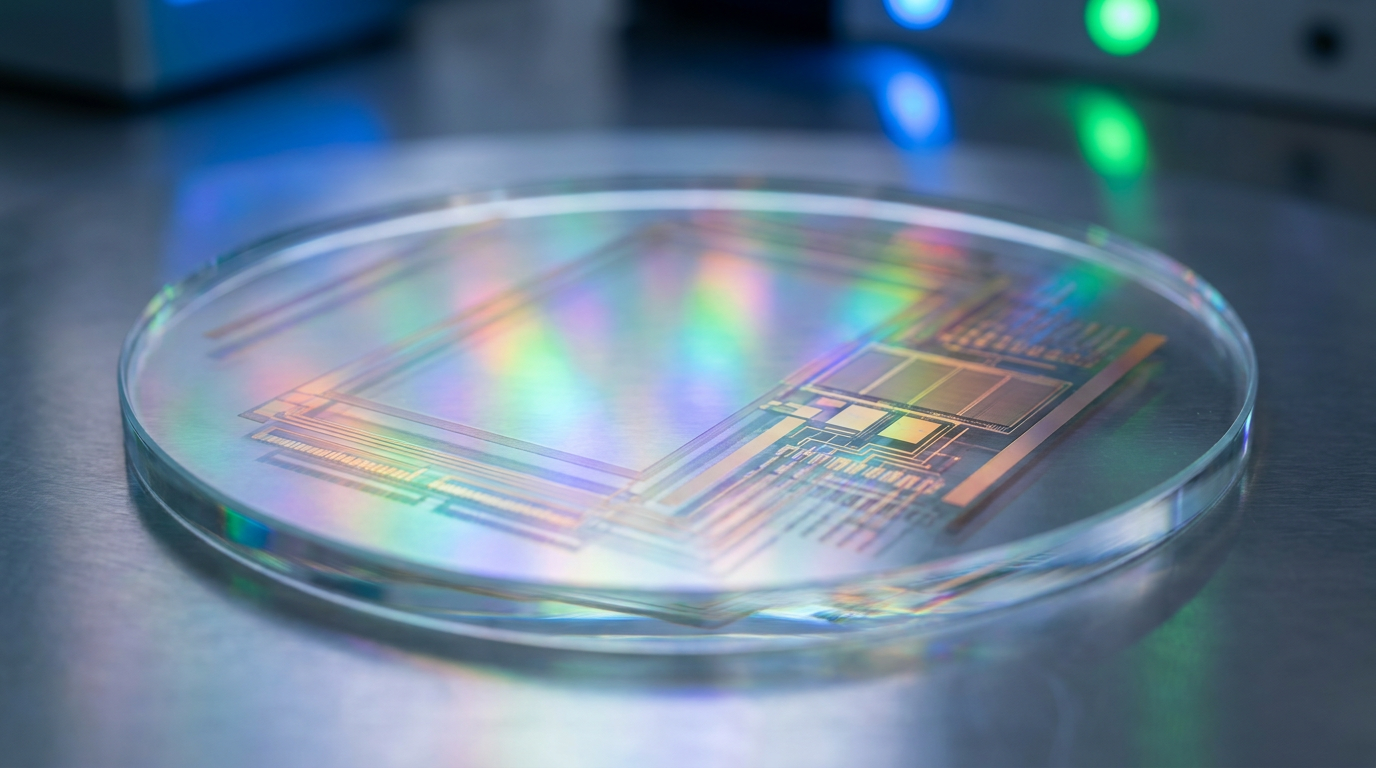
The solution, which has quietly become one of the most important breakthroughs in modern computing, is glass. Specifically, the industry is racing to commercialize "glass core substrates" (GCS). By replacing the organic core of the chip package with ultra-flat, thermally stable borosilicate or quartz glass, engineers can fundamentally rewrite the rules of semiconductor design.[1]

The physical benefits of glass are staggering. According to Semiconductor Engineering, glass boasts 50% less warpage and 35% better positional accuracy than traditional organic cores. Because it barely expands or contracts under heat, glass allows manufacturers to etch microscopic wiring with unprecedented precision.[4]
In traditional organic substrates, the tiny copper wires that route power and data struggle to get smaller than a few microns without short-circuiting. Glass, with its perfectly smooth surface, enables sub-2-micron lines and spaces. This allows for up to 10 times the interconnect density, meaning chips can talk to each other faster and with far less energy.[4]
The performance gains are not theoretical. ResearchAndMarkets projects that glass substrates can deliver up to a 40% improvement in processing speeds while cutting power consumption in half compared to conventional organic materials. For data centers consuming gigawatts of electricity to train AI models, that efficiency is transformative.[3]
For data centers consuming gigawatts of electricity to train AI models, that efficiency is transformative.
Furthermore, glass possesses a dielectric constant much lower than silicon, meaning electrical signals experience significantly less transmission loss. This makes glass an ideal medium not just for AI processors, but for high-frequency 6G communications and silicon photonics, where data is transmitted via light rather than electricity.[4]
Recognizing this paradigm shift, the world's largest technology companies are aggressively pivoting. Intel, which committed to glass substrates in its advanced packaging roadmap in 2023, recently debuted a massive 78x77-millimeter glass-core package at the NEPCON Japan 2026 conference. The prototype demonstrated a flawless structure with zero micro-cracks, marking a decisive step toward commercial reality.[2]

Meanwhile, South Korea is mobilizing massive capital to capture the market. SKC recently approved a $690 million capital increase, directing over $400 million to its US-based subsidiary, Absolics. Absolics is already ramping up prototype production at a new facility in Georgia, aiming to supply global Big Tech clients with glass substrates for AI data centers.[6]
Samsung Electro-Mechanics (SEMCO) is also accelerating its timeline, having established a pilot line in Sejong and delivered its first samples to major clients. The competitive intensity is surging, with IDTechEx reporting that glass is rapidly moving "from a background consumable to the heart of a package."[5][6]
The transition is also reshaping semiconductor geopolitics. The "chip war" between the United States and China has historically focused on restricting access to advanced lithography machines that print transistors. But as the bottleneck shifts from the silicon die to the packaging substrate, control over the glass supply chain is becoming a critical national security priority.[1]
Industry analysts note that advanced packaging facilities capable of glass core production require investments approaching $1 billion. With state-backed funds pouring capital into domestic packaging specialists globally, the race to dominate glass substrates could dictate which nation ultimately controls the infrastructure of artificial intelligence.[1]
Despite the immense promise, commercializing glass at scale presents formidable manufacturing challenges. Glass is inherently brittle. Handling ultra-thin, 100-micron glass panels in automated cleanrooms without shattering them requires entirely new equipment and handling protocols.[1]

Additionally, drilling the microscopic holes through the glass—known as Through-Glass Vias (TGVs)—requires highly specialized laser processing and chemical etching. Filling these microscopic glass tunnels with copper without leaving voids is a metallurgical hurdle that materials companies are still refining.[4]
Yet, the trajectory is clear. A recent report by SEMI and Global Net Corp. forecasts that the glass core substrate market will see a staggering compound annual growth rate (CAGR) of 67.2% between 2028 and 2040. As traditional device scaling slows, glass has emerged not just as an alternative, but as the mandatory foundation for the next generation of computing.[7]
How we got here
2023
Intel officially commits to glass substrates in its advanced packaging roadmap, signaling a major industry shift.
Early 2024
Samsung Electro-Mechanics formally declares its entry into the glass substrate market and establishes a pilot line.
January 2026
Intel debuts a flawless 78x77mm glass-core package prototype at NEPCON Japan, proving the technology's viability.
February 2026
SKC approves a $690 million capital increase to accelerate mass production at its Absolics facility in Georgia.
Viewpoints in depth
Industry Analysts' View
Market researchers view glass substrates as the inevitable successor to organic materials, driven purely by the physical demands of AI scaling.
Forecasters from SEMI and TrendForce emphasize that traditional organic substrates have simply run out of runway. As AI accelerators grow larger to accommodate more compute cores, the heat generated causes organic materials to warp, destroying yields. Analysts project that the transition to glass is not just an optional upgrade but a mandatory evolution, forecasting explosive growth rates exceeding 60% annually as data centers demand the 40% speed boosts and 50% power reductions that glass enables.
Materials Engineers' View
Engineers focus on the immense technical hurdles of handling and metallizing ultra-thin glass at mass-production scales.
While the electrical and thermal properties of glass are vastly superior, materials experts highlight the fragility of the medium. Drilling tens of thousands of microscopic Through-Glass Vias (TGVs) without fracturing the 100-micron-thick panels requires bleeding-edge laser technology. Furthermore, ensuring that copper plating adheres perfectly to the smooth glass walls inside these vias remains a complex metallurgical challenge that the industry is still actively solving.
Geopolitical Observers' View
Strategic analysts view advanced packaging as the new frontline in the global semiconductor cold war.
With the US heavily restricting China's access to advanced transistor lithography, geopolitical observers note that the battleground has shifted to packaging. Because glass substrates allow older, larger chips to be stitched together to rival the performance of cutting-edge silicon, controlling the glass supply chain is a matter of national security. Observers track the massive capital deployments by South Korean firms like SKC and state-backed Chinese funds as a race to secure the infrastructure of future AI dominance.
What we don't know
- Whether the industry can reduce the manufacturing costs of glass substrates enough to make them viable for consumer electronics, rather than just premium AI servers.
- How quickly the supply chain for specialized glass-handling equipment can scale to meet the projected 67% annual market growth.
- Which specific metallization and laser-drilling techniques will emerge as the dominant industry standard for Through-Glass Vias (TGVs).
Key terms
- Organic Substrate
- The traditional plastic-like foundational layer in a chip package that routes electrical signals, which is now reaching its thermal and physical limits.
- Glass Core Substrate (GCS)
- A next-generation chip packaging technology that replaces the organic core with ultra-flat glass, enabling higher interconnect density and better heat resistance.
- Through-Glass Via (TGV)
- Microscopic vertical tunnels drilled through the glass substrate using lasers, filled with metal to connect different layers of the microchip.
- Advanced Packaging
- The process of combining multiple smaller chips (chiplets) into a single, high-performance system, rather than printing one massive silicon die.
- Redistribution Layer (RDL)
- The microscopic copper wiring network within a substrate that routes power and data between the silicon chip and the main circuit board.
Frequently asked
Why are chipmakers switching to glass substrates?
Modern AI chips generate immense heat, causing traditional organic substrates to warp and fail. Glass remains perfectly flat under high temperatures and allows for much denser, faster electrical connections.
When will glass substrates be in consumer devices?
Initial mass production is targeting high-end AI data centers and supercomputers starting in 2026. It will likely take several more years before the technology scales down to consumer laptops and smartphones.
Does this mean silicon chips are going away?
No. The actual processing chips are still made of silicon. Glass is replacing the 'substrate'—the foundational board that the silicon chips sit on and communicate through.
Who is leading the race to manufacture glass substrates?
Intel is a major pioneer in the research, while South Korean companies like SKC (through its US subsidiary Absolics) and Samsung Electro-Mechanics are racing to be the first to achieve high-volume mass production.
Sources
Source coverage
7 outlets
3 viewpoints surfaced


[1]Factlen Editorial TeamCorporate & Geopolitical Observers
Synthesis by Factlen editorial team
Read on Factlen Editorial Team →[2]TrendForceIndustry Analysts & Forecasters
Glass Substrates: The Next-Generation Material for Advanced Packaging
Read on TrendForce →[3]ResearchAndMarketsIndustry Analysts & Forecasters
The Global Market for Glass Substrates for Semiconductors 2026-2036
Read on ResearchAndMarkets →[4]Semiconductor EngineeringEngineering & Materials Experts
Glass Substrates Gain Traction in Advanced Packaging
Read on Semiconductor Engineering →[5]IDTechExIndustry Analysts & Forecasters
Glass in Semiconductors 2026-2036: Applications, Emerging Technologies, and Market Insights
Read on IDTechEx →[6]Economy.acCorporate & Geopolitical Observers
Competition among domestic and global companies is intensifying over the commercialization of glass core substrates
Read on Economy.ac →[7]SEMIIndustry Analysts & Forecasters
Glass Core Substrate Market and Development Trends
Read on SEMI →
Every angle. Every day.
Get technology stories with full source coverage and perspective breakdowns delivered to your inbox.