How Glass Substrates Are Solving the AI Industry's Biggest Hardware Bottleneck
As artificial intelligence processors grow larger and run hotter, traditional plastic foundations are reaching their physical limits. Now, the semiconductor industry is turning to engineered glass to build the next generation of ultra-powerful chips.
By Factlen Editorial Team
- Advanced Foundry Leaders
- Major chipmakers view glass as the inevitable next step for scaling AI performance.
- Material & Display Innovators
- Glass and display giants see a unique opportunity to enter the lucrative semiconductor supply chain.
- Packaging Analysts & Skeptics
- Industry observers caution that the manufacturing hurdles for glass are still immense.
What's not represented
- · Environmental groups monitoring glass recycling
- · Consumer electronics brands waiting for cost reductions
Why this matters
The shift to glass substrates is one of the most significant material changes in semiconductor manufacturing in decades. It will enable the massive leaps in computing power required for future AI, 6G networks, and advanced autonomous systems.
Key points
- AI processors are outgrowing traditional plastic substrates, which warp under extreme heat.
- Engineered glass cores offer superior rigidity, thermal stability, and signal integrity.
- Glass allows for up to 10 times the connection density of organic materials.
- Major foundries and display manufacturers are racing to commercialize the technology by 2026-2028.
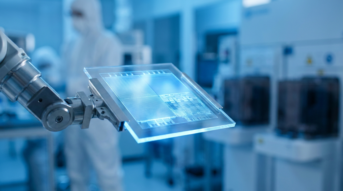
The artificial intelligence infrastructure buildout is often discussed in terms of chips and computing power, but beneath the surface, a quiet revolution is happening in the materials that hold those chips together. As AI models demand unprecedented data throughput, the physical processors are growing larger and running hotter than ever before.[1]
Every advanced chip rests on a foundational platform called a substrate, which connects its microscopic, hair-thin wiring to the coarser circuitry of the main motherboard. For decades, this platform has been built from layers of organic plastic resin, commonly known as ABF (Ajinomoto Build-up Film).[3]
It is a system that has worked brilliantly for years, but it is now hitting a physical wall. As AI accelerators expand in size and generate immense heat, the plastic resin tends to warp—bending much like a wooden table in a damp room. This warpage distorts the microscopic signals it is meant to carry, reducing manufacturing yields and limiting how large a chip package can physically become.[1][3]
Enter the glass core substrate. By replacing the organic plastic core with engineered glass, the semiconductor industry is unlocking a new era of advanced packaging. Glass does not bend under extreme thermal stress; it stays perfectly flat, holding its dimensional shape with the rigidity of steel.[2][3]

This is not standard window glass or smartphone screen material. It is a highly engineered, specialized formulation—often borosilicate or alkali-free aluminosilicate glass—designed to precisely match the thermal expansion properties of the silicon chips that sit on top of it.[6][7]
The architecture of a glass substrate is essentially a high-tech sandwich. A central glass core, typically measuring between 100 and 500 micrometers thick, sits in the middle. Traditional organic build-up layers and copper wiring are then stacked on both the top and bottom surfaces of this rigid glass foundation.[6][8]
The magic happens inside the glass itself through a technology called Through-Glass Vias (TGVs). Using highly precise lasers, manufacturers drill microscopic holes through the glass core and plate them with copper. These TGVs act as vertical electrical highways, allowing data and power to flow seamlessly through the package.[2]
Because glass is exceptionally smooth and dimensionally stable, these vias and the surrounding wiring can be packed much closer together. Industry experts note that glass substrates can achieve up to 10 times the interconnect density of traditional organic materials.[8]

Because glass is exceptionally smooth and dimensionally stable, these vias and the surrounding wiring can be packed much closer together.
Beyond density, glass offers vastly superior electrical performance. It features a significantly lower dielectric constant and lower signal loss compared to plastic. For the ultra-fast 112 Gbps signaling rates required by next-generation AI accelerators and 6G communications, this means data travels faster, cleaner, and with less power consumption.[1][6][7]
The realization of these physical limits has triggered a massive, multi-billion-dollar race among the world's top technology companies. Intel has been a pioneer in this space, investing heavily over the last decade and committing to mass production of glass substrates in the latter half of the 2020s.[1][2]
South Korea is aggressively pursuing the technology as well. SKC's subsidiary, Absolics, has built a dedicated manufacturing plant in Covington, Georgia, backed by U.S. CHIPS Act funding, with the sole purpose of mass-producing glass substrates. Meanwhile, Samsung Electronics and LG Innotek are rapidly developing their own pilot lines to ensure they do not fall behind in the AI hardware race.[3][5]
TSMC, the world's dominant foundry, is also advancing its own glass-based architecture. Reports indicate TSMC is developing a "Chip-on-Panel-on-Substrate" (CoPoS) technology utilizing glass, targeting ultra-large packages for future AI chips, with mass production slated for the 2026 to 2028 timeframe.[9]

The shift to glass has also opened a unique backdoor for companies outside the traditional semiconductor supply chain. Display panel giants, who have spent decades mastering the handling and processing of large glass sheets for televisions and smartphones, are now pivoting into chip packaging. Companies like China's BOE and glass specialists like SCHOTT and Corning are leveraging their deep material expertise to supply the foundational sheets.[4][7]
Despite the immense promise, commercializing glass substrates at scale is an engineering nightmare. The primary challenge is the inherent brittleness of the material. A modern substrate manufacturing process can involve nearly 190 distinct steps, and a microscopic crack formed early in the process can cause the entire panel to shatter during later testing or assembly.[2][3]
Metallization presents another steep hurdle. Because glass is so smooth, getting copper to adhere to the walls of the microscopic TGVs without leaving voids or bubbles pushes the limits of current electroplating chemistry. A single void in a copper via becomes an electrical weak point that can ruin an entire AI processor.[4]
To solve this, the equipment ecosystem is rapidly evolving. Laser companies are developing new "laser-induced deep etching" techniques that modify the glass structure before chemical etching, creating perfectly shaped holes that are easier to fill with metal.[2][6]

Market analysts project that the global market for glass in semiconductors will reach $4.4 billion by 2036, representing a massive shift in the supply chain. While organic substrates will remain the standard for cost-sensitive, everyday electronics, glass is poised to take over the high-performance computing sector.[1][6]
As the demand for artificial intelligence continues to outpace the capabilities of traditional hardware, the foundation of computing must evolve. By swapping plastic for glass, the semiconductor industry is ensuring that the physical limits of materials do not bottleneck the future of technology.[7]
How we got here
2023
Intel publicly commits to introducing glass substrates for advanced packaging in the latter half of the decade.
2024
The U.S. government awards Absolics $75 million under the CHIPS Act to build a glass substrate facility in Georgia.
2025
Major display panel manufacturers and foundries begin establishing pilot lines for glass core substrates.
2026-2028
Anticipated window for the first wave of mass-produced glass substrates to enter the AI hardware market.
Viewpoints in depth
Advanced Foundry Leaders
Major chipmakers view glass as the inevitable next step for scaling AI performance.
For companies like Intel, TSMC, and Samsung, the physical limits of organic substrates represent a hard ceiling on Moore's Law. They argue that to build the massive, multi-chiplet processors required for next-generation AI, the industry must transition to a perfectly flat, thermally stable foundation. Their primary focus is on driving down defect rates and scaling up manufacturing throughput to make glass economically viable.
Material & Display Innovators
Glass and display giants see a unique opportunity to enter the lucrative semiconductor supply chain.
Companies that have spent decades perfecting the mass production of LCD and OLED panels—such as BOE, Corning, and SCHOTT—are uniquely positioned for this shift. They argue that their deep expertise in handling ultra-thin, fragile glass sheets gives them a structural advantage. For these firms, glass substrates represent a highly profitable backdoor into the advanced packaging market, allowing them to bypass traditional silicon manufacturing entirely.
Packaging Analysts & Skeptics
Industry observers caution that the manufacturing hurdles for glass are still immense.
While acknowledging the superior physics of glass, skeptics point to the brutal realities of the factory floor. They highlight that a single microscopic crack during a 190-step manufacturing process can shatter an entire panel. Furthermore, getting copper to adhere perfectly to the smooth walls of a Through-Glass Via (TGV) without leaving voids remains a severe chemical challenge. This camp warns that true commercialization at scale may take longer than the optimistic 2026-2028 targets.
What we don't know
- Whether the industry can reduce the microcracking defect rate enough to make glass substrates cost-competitive.
- Which specific laser-etching technology will become the industry standard for drilling Through-Glass Vias.
- How quickly the technology will trickle down from high-end AI servers to consumer-grade electronics.
Key terms
- Substrate
- The foundational layer that connects a microscopic semiconductor chip to the main circuit board of a computer.
- Chiplet
- A small, specialized chip designed to be combined with others in a single package to form a larger, more powerful processor.
- Organic Substrate (ABF)
- The current industry standard foundation made of resin and fiberglass, which is prone to warping under extreme heat.
- Through-Glass Via (TGV)
- Microscopic holes drilled through a glass core and filled with metal to carry electrical signals vertically through the package.
- Warpage
- The bending or distortion of a chip package caused by uneven thermal expansion, which can break delicate electrical connections.
Frequently asked
Why can't we just keep using plastic substrates?
As AI chips grow larger and run hotter, traditional plastic (organic) substrates warp under the heat. This bending breaks microscopic connections and limits how large a processor can be built.
Is this the same glass used in smartphone screens?
No. It is a highly engineered, specialized formulation—such as borosilicate or alkali-free aluminosilicate—designed specifically to match the thermal expansion properties of silicon.
When will glass substrates be in consumer devices?
Mass production is targeted between 2026 and 2028. However, they will initially be used in high-end AI data center chips and 6G infrastructure before trickling down to consumer electronics.
Will glass completely replace organic substrates?
Unlikely. Organic substrates will remain the standard for cost-sensitive, everyday electronics, while glass will dominate the high-performance computing sector where its premium cost is justified.
Sources
Source coverage
9 outlets
3 viewpoints surfaced


[1]TrendForceAdvanced Foundry Leaders
Glass Substrates Are Breaking Through the AI Chip Packaging Bottleneck
Read on TrendForce →[2]Semiconductor EngineeringPackaging Analysts & Skeptics
The Race To Glass Substrates
Read on Semiconductor Engineering →[3]The Korea HeraldMaterial & Display Innovators
Korea's hidden AI race is made of glass
Read on The Korea Herald →[4]PandailyMaterial & Display Innovators
Glass Core Substrates Are Booming: How Far Are They From True Commercialization in Chip Packaging?
Read on Pandaily →[5]SemiWikiAdvanced Foundry Leaders
Samsung Electronics and Intel explore a foundry alliance, joining forces on everything from packaging to glass substrates
Read on SemiWiki →[6]IDTechExPackaging Analysts & Skeptics
Glass in Semiconductors 2026-2036: Applications, Emerging Technologies, and Market Insights
Read on IDTechEx →[7]SCHOTTMaterial & Display Innovators
Beyond speed: what glass-based chips mean for the devices of tomorrow
Read on SCHOTT →[8]Future Markets IncPackaging Analysts & Skeptics
The Global Market for Glass Substrates for Semiconductors 2026-2036
Read on Future Markets Inc →[9]Sammy FansAdvanced Foundry Leaders
TSMC develops glass-based CoPoS packaging as Samsung advances HPB for AI chips
Read on Sammy Fans →
More in technology
See all 5 stories →


Every angle. Every day.
Get technology stories with full source coverage and perspective breakdowns delivered to your inbox.