
Intel Foundry Unveils Hyper-Large Chip Packaging Blueprint to Scale AI Training Systems
Intel has detailed a new advanced packaging architecture that bypasses traditional manufacturing limits, allowing AI chips to scale to unprecedented sizes. The breakthrough in "encapsulation" enables massive, multi-chiplet systems that could power the next generation of AI data centers.
By Mateo Ramos


- Foundry Innovators
- Focus on pushing the physical boundaries of semiconductor manufacturing and advanced packaging to enable next-generation AI.
- AI Infrastructure Architects
- View packaging as the new strategic battleground for AI accelerator cost structures, yield, and system performance.
- Semiconductor Analysts
- Highlight the competitive dynamics, noting how Intel's open foundry model and US-based packaging capacity challenge existing supply chains.
Why this matters
As AI models grow exponentially, they require hardware that exceeds the physical limits of traditional chip manufacturing. By successfully stitching together dozens of chips into a single massive package, this breakthrough ensures the continued scaling of AI capabilities and reshapes the economics of data center infrastructure.
Key points
- Intel Foundry detailed plans for Hyper-Large Form Factor (HLFF) packages measuring up to 240 by 240 millimeters.
- The architecture bypasses the traditional 'reticle limit' by stitching dozens of chiplets together into a single system.
- Engineers solved a major manufacturing hurdle by developing new materials to encapsulate massive chips without air voids.
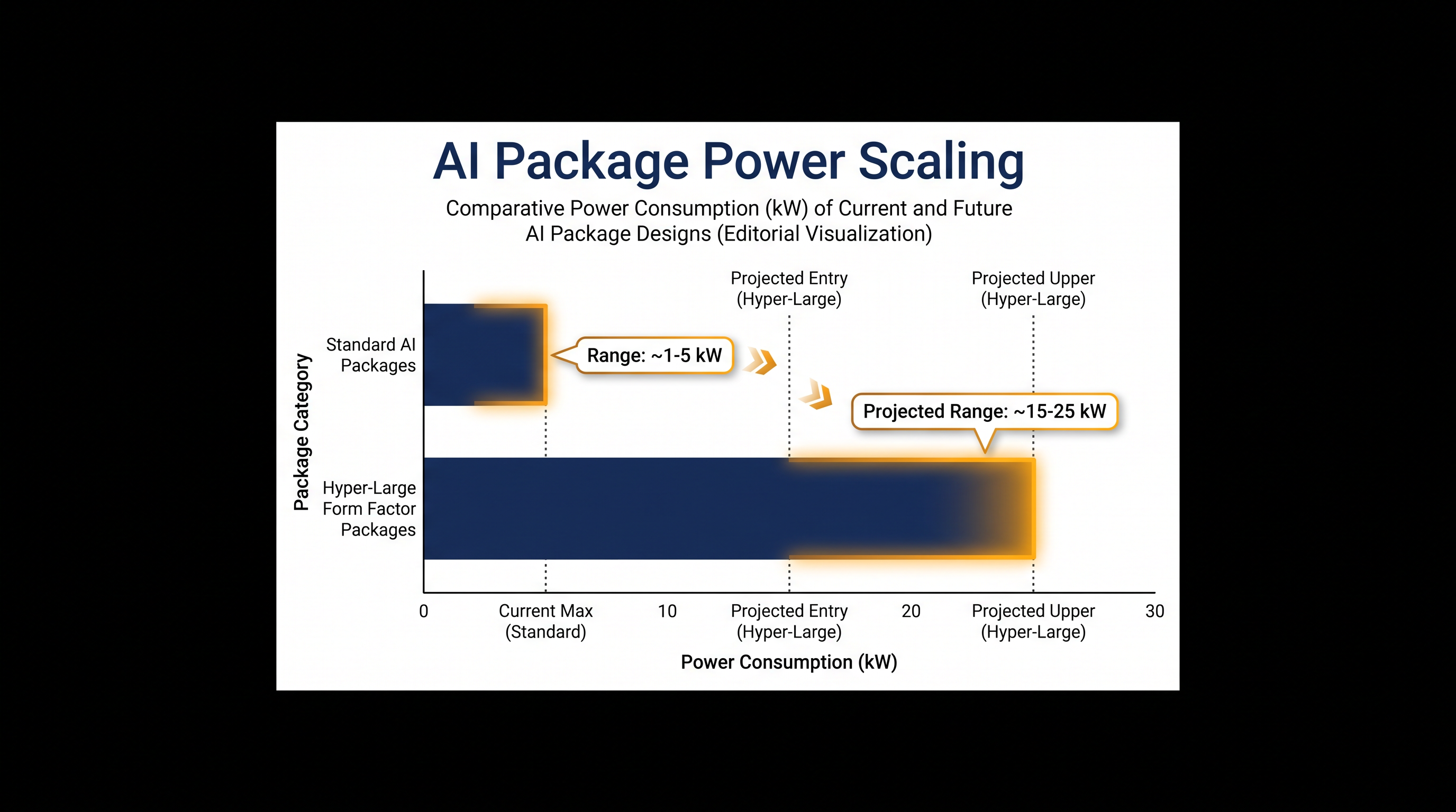
- The massive packages are projected to draw 15 to 25 kilowatts of power, requiring modular cell-based cooling architectures.
As artificial intelligence models grow exponentially in size and complexity, the physical hardware required to train them is hitting a fundamental wall. For decades, the semiconductor industry relied on shrinking transistors to pack more power into a single silicon die. But today's frontier AI workloads demand unprecedented compute density, pushing single chips to their maximum printable size—a manufacturing boundary known as the reticle limit.[1][2]
To bypass this physical constraint, the industry is shifting from monolithic chips to "chiplets"—specialized tiles of silicon stitched together to function as a single, massive brain. At the 2026 IEEE Electronic Components and Technology Conference (ECTC), Intel Foundry unveiled a comprehensive blueprint for the next generation of these systems, detailing "hyper-large form factor" (HLFF) packages that dwarf anything currently on the market.[1][3]
The newly detailed HLFF architecture aims to scale AI chip packages to a staggering 240 by 240 millimeters. To put that into perspective, this achieves a 24x reticle size—meaning the combined silicon area is 24 times larger than the maximum size a standard lithography machine can print in a single exposure.
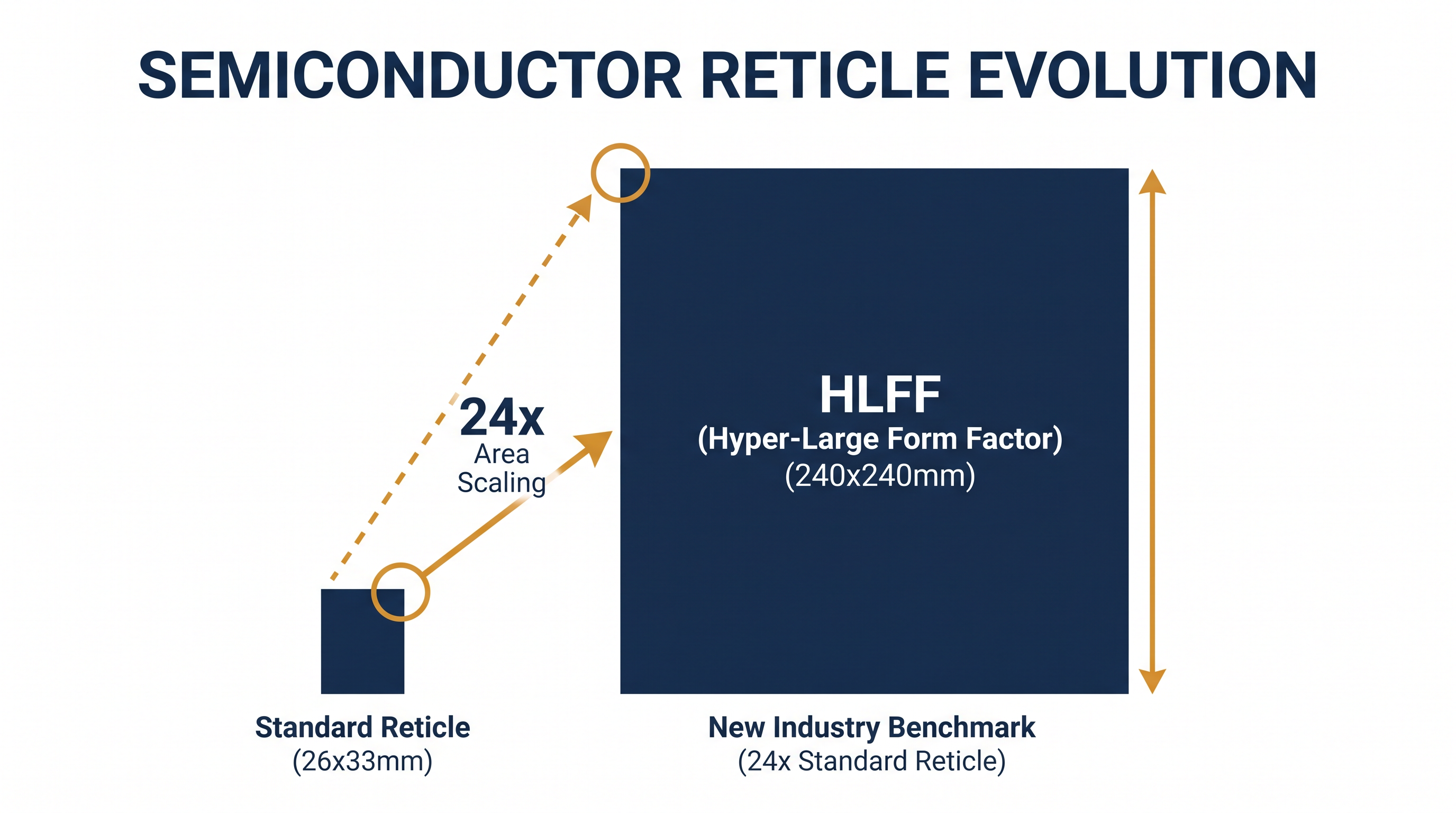
"We've moved past the era of one big chip to a system of chips, almost like a silicon mosaic," explained Katie Prouty, manager of Intel's Fab 9 advanced packaging facility in Rio Rancho, New Mexico. This facility has become the epicenter of Intel's U.S.-based advanced packaging efforts, transforming from a legacy wafer fab into a critical hub for next-generation AI hardware.[2]
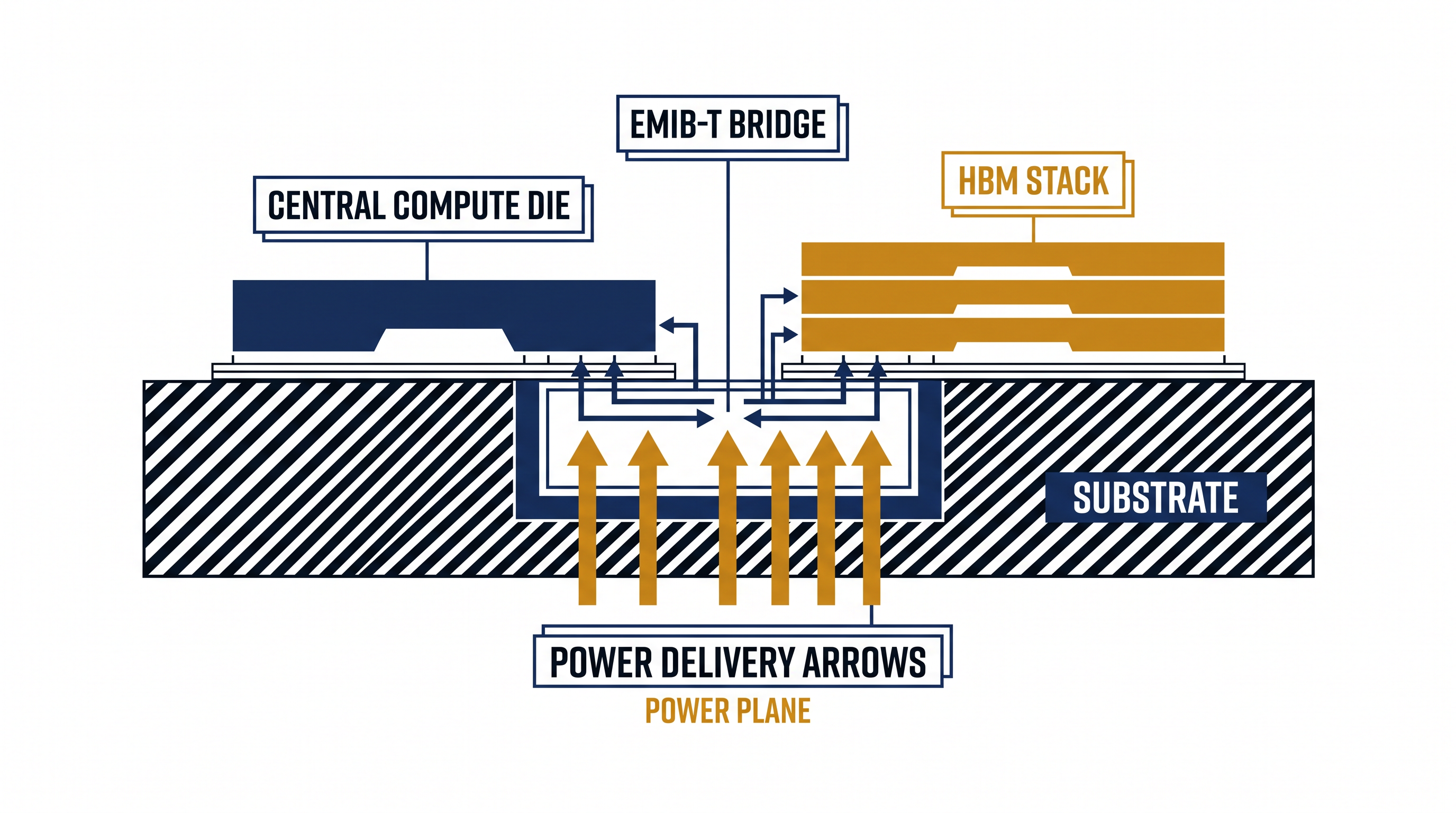
Building a package of this magnitude requires more than just placing chips side-by-side; they must communicate with zero bottleneck. Intel's solution relies heavily on its Embedded Multi-die Interconnect Bridge (EMIB) technology. Instead of using a massive, expensive silicon interposer as a foundational layer, EMIB embeds tiny, high-speed silicon bridges directly into the organic substrate only where connections are needed.[1][2]
The latest iteration, EMIB-T, takes this a step further by adding vertical channels through the bridge itself. This allows power to be delivered directly to the compute dies and high-bandwidth memory (HBM) from below, rather than routing it around the interconnects. This vertical power delivery is crucial for maintaining signal integrity and power efficiency in systems that integrate dozens of distinct silicon tiles.[1]
However, designing a massive package on a whiteboard is entirely different from manufacturing it reliably. As Intel's Advanced Design team pushed the architectural boundaries, the Assembly Technology Development team had to solve a critical manufacturing roadblock: encapsulation.
Encapsulation is the process of injecting a protective "underfill" material between the chiplets and the substrate to protect the microscopic solder bumps from thermal and mechanical stress. In standard packages, this liquid material only needs to flow about 22 millimeters. In hyper-large packages, it must travel up to 43 millimeters through a dense forest of connections.
In standard packages, this liquid material only needs to flow about 22 millimeters.
"When you talk about 5x-10x reticle scales, the underfill has to reach much larger distances," industry analysts noted, explaining that the increased distance adds resistance, making it incredibly difficult to remove air pockets and voids. A single microscopic void in the underfill can cause the entire multi-thousand-dollar AI package to fail under the intense heat of operation.
Intel Foundry solved this encapsulation wall through three coordinated levers: material chemistry, dispensing strategy, and curing processes. Engineers developed a new underfill formulation with significantly lower viscosity, allowing it to flow further without sacrificing the mechanical rigidity required to protect the chips.
Combined with a redesigned dispensing strategy, Intel successfully validated void-free encapsulation on test vehicles exceeding 5x and 7x reticle sizes. One test chip housed 18 separate dies, including 12 HBM sites, achieving perfect encapsulation at flow distances of up to 40 millimeters.
With the physical manufacturing constraints addressed, the next hurdle for these hyper-large packages is thermal management. Intel projects that fully realized HLFF packages will consume between 15 and 25 kilowatts (kW) of power each.
Dissipating that much heat from a concentrated area requires a radical departure from traditional data center cooling. Instead of a single massive cold plate, Intel's blueprint proposes a modular, cell-based cooling architecture featuring independently controlled thermal zones and embedded sensors, designed to scale beyond 5 kW of cooling per individual module.
The implications of this packaging blueprint extend far beyond Intel's own product lines. As an "Open System Foundry," Intel is offering these advanced packaging services to external customers, allowing AI accelerator designers to mix and match chiplets from different foundries—including TSMC or Samsung—onto Intel's massive substrates.[1]
This flexibility is reshaping the economics of AI hardware. According to market research firm The Futurum Group, packaging architecture is becoming a "central determinant of what next-generation AI accelerators can achieve." By shifting from monolithic designs to modular chiplets, companies can dramatically improve manufacturing yields and lower cost structures.[3]
The ecosystem is already aligning around these new capabilities. Electronic Design Automation (EDA) giants like Cadence and Synopsys have certified their AI-driven design flows for Intel's latest nodes and advanced packaging technologies, giving chip architects a trusted path to design these massive systems.
Looking ahead, Intel Foundry is already researching the next bottlenecks. Engineers are developing glass core substrates to replace traditional organic materials, offering better power stability and lower warpage for massive packages. They are also pioneering co-packaged optics (CPO), which will move optical-to-electrical signal conversion directly onto the package to handle the immense bandwidth demands of future AI clusters.[1]
For now, the breakthrough in hyper-large encapsulation marks a critical milestone. By successfully scaling past the reticle limit, the semiconductor industry has secured the hardware runway necessary to train the next generation of frontier AI models, ensuring that physical manufacturing limits will not stall the pace of artificial intelligence research.[3]
How we got here
1980s
Intel's Rio Rancho facility leads the industry in 6-inch wafer manufacturing.
May 2026
Intel presents HLFF package architectures and encapsulation solutions at the ECTC conference.
July 2026
Intel details EMIB-T technology and its ability to bypass the reticle limit for AI workloads.
2028 (Projected)
Advanced packaging is expected to scale beyond 12x the industry standard reticle limit.
Viewpoints in depth
Foundry Innovators
Focus on the physical engineering required to overcome the reticle limit and encapsulation physics.
For semiconductor engineers, the primary challenge of the AI boom is physical space. Because lithography machines can only print silicon up to a certain size, the only way to build a more powerful AI brain is to stitch multiple chips together. Foundry innovators view breakthroughs like low-viscosity underfill and vertical power delivery as the unsung heroes of the AI revolution, arguing that without these material science advancements, software progress would soon hit a hard hardware ceiling.
AI Infrastructure Architects
Focus on how modular chiplets improve yield and demand entirely new data center cooling paradigms.
System architects view hyper-large packaging as a double-edged sword. On one hand, breaking a massive AI accelerator into smaller chiplets drastically improves manufacturing yields and lowers costs, as a single defect no longer ruins the entire processor. On the other hand, concentrating 15 to 25 kilowatts of power into a 240-millimeter square creates unprecedented thermal density. These architects argue that realizing the potential of HLFF packages will require data centers to completely abandon traditional air cooling in favor of aggressive, direct-to-chip liquid cooling modules.
Semiconductor Analysts
Focus on how Intel's open foundry model and US-based packaging capacity offer an alternative to constrained supply chains.
Market analysts view Intel's packaging blueprint through a geopolitical and competitive lens. With the AI industry heavily reliant on TSMC's CoWoS (Chip-on-Wafer-on-Substrate) packaging—which has faced severe supply bottlenecks—Intel's ability to offer hyper-large packaging from its New Mexico facilities provides a crucial alternative. Analysts note that by allowing customers to bring chiplets manufactured at rival foundries and package them on Intel substrates, Intel is positioning itself as an indispensable middleman in the global AI hardware supply chain.
What we don't know
- How quickly external AI accelerator companies will adopt Intel's 240x240mm packaging standard.
- The exact cost per unit of manufacturing these hyper-large packages at scale.
- Whether existing data center infrastructure can be retrofitted to handle the 15-25kW thermal density of these new systems.
Key terms
- Reticle Limit
- The maximum physical area that a semiconductor lithography tool can expose in a single step, traditionally capping how large a single silicon chip can be.
- Chiplet
- A smaller, specialized integrated circuit designed to be combined with others within a single package to form a larger, more complex system.
- EMIB-T
- Embedded Multi-die Interconnect Bridge-T, an Intel technology that embeds tiny silicon bridges in the substrate to connect chiplets and deliver power vertically.
- Encapsulation
- The process of sealing chips onto a package with a protective underfill material to ensure mechanical integrity and protect against thermal stress.
- Co-Packaged Optics (CPO)
- Integrating optical-to-electrical signal conversion directly onto the chip package to dramatically increase bandwidth and reduce power consumption.
Frequently asked
Why can't we just make larger single chips for AI?
Semiconductor manufacturing is constrained by the "reticle limit," the maximum size a lithography machine can print at once. To build larger systems, manufacturers must stitch multiple smaller chips together.
What was the main barrier to building these hyper-large packages?
Encapsulation. Flowing protective underfill material across massive distances without creating microscopic air voids was a major physical challenge that required new materials and dispensing strategies.
How much power will these new AI packages consume?
Intel projects that hyper-large form factor (HLFF) packages will operate at 15 to 25 kilowatts, requiring advanced modular cooling architectures to prevent overheating.
Sources
Source coverage
3 outlets
3 viewpoints surfaced



[1]Intel NewsroomFoundry Innovators
Intel's U.S. Advanced Packaging Enables Next-Generation AI Semiconductors
Read on Intel Newsroom →[2]Design And ReuseSemiconductor Analysts
How Intel Foundry uses Foveros stacking, EMIB silicon bridges, and EMIB-T to scale chiplets
Read on Design And Reuse →[3]The Futurum GroupAI Infrastructure Architects
Packaging the AI Frontier: Intel Foundry's Advanced Packaging Alignment with the XPU Industry Roadmap
Read on The Futurum Group →
Comments

Every angle. Every day.
Get ai stories with full source coverage and perspective breakdowns delivered to your inbox.