
How Stacking DRAM Over Silicon Interposers Trades Clock Frequency for a 1,024-Bit Bus Width
By replacing narrow, high-frequency data channels with massive parallel pathways, advanced 2.5D packaging slashes the energy required to move memory bits by over 40 percent. This architectural shift allows artificial intelligence accelerators to bypass the thermal limits of traditional circuit boards.

In short
- Silicon interposers enable ultra-wide 1,024-bit memory buses that cannot be physically routed on traditional printed circuit boards.
- By moving data across thousands of parallel lanes, High Bandwidth Memory achieves massive throughput at significantly lower clock frequencies.
- This spatial parallelism reduces the energy required to move a single bit of data by over 40 percent compared to conventional graphics memory.
Modern artificial intelligence models now process terabytes of data per second, fundamentally breaking the energy limits of traditional computer memory. To prevent processors from melting under the power demands of high-speed data transfer, the semiconductor industry has abandoned conventional memory boards in favor of stacking memory chips directly onto silicon interposers.[4]
This architectural shift replaces narrow, high-frequency data buses with massive 1,024-bit parallel pathways. By trading clock speed for physical width, engineers have successfully slashed the energy required to move a single bit of data by over 40 percent.[1][4]
The transition from standard graphics memory to High Bandwidth Memory (HBM) represents a complete reimagining of how data travels. Instead of forcing bits through a narrow pipe at extreme frequencies, the interposer architecture moves thousands of bits simultaneously at a much slower, cooler pace.[2]
The Memory Wall and the Frequency Trap
For decades, the standard approach to increasing memory bandwidth was simply to drive the clock frequency higher. Traditional memory modules, such as Double Data Rate (DDR) or Graphics Double Data Rate (GDDR), rely on relatively narrow data buses—typically 32 or 64 bits wide.
To feed increasingly hungry processors, these narrow buses had to operate at blistering speeds. Modern GDDR6X configurations, often used in consumer graphics cards, require data rates of up to 23 gigabits per second per pin just to maintain acceptable throughput.[1]
However, pushing electrical signals at these frequencies across a standard printed circuit board requires immense power. As clock speeds escalate, the energy required to maintain signal integrity and overcome electrical resistance grows exponentially across the entire system.[1][2]
This phenomenon, often referred to as the memory wall, meant that high-performance processors were spending more energy moving data than actually computing it. In high-end graphics and AI training workloads, this temporal frequency scaling became thermally unsustainable.[2]
Engineers realized that continuing to accelerate the clock rate would eventually cause the memory interface to consume the entire power budget of the server. A radically different approach was required to decouple bandwidth from frequency.[2][3]
The Silicon Interposer Solution
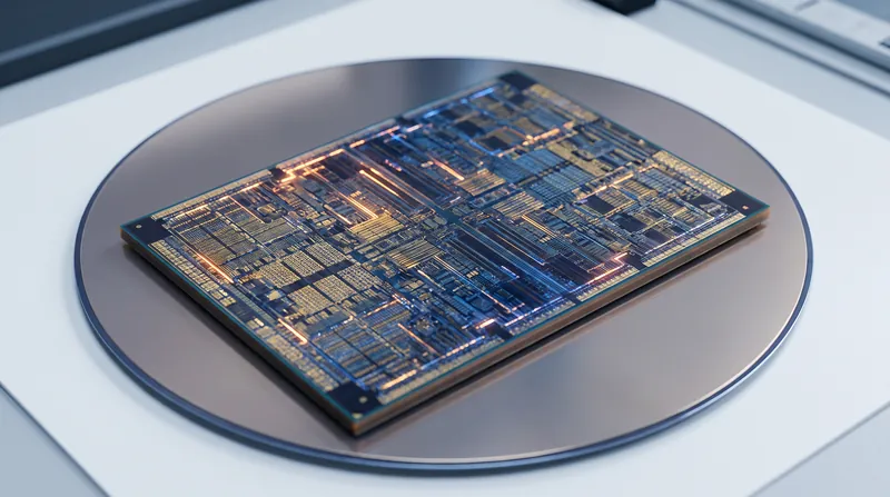
To break the frequency trap, designers introduced the silicon interposer, a foundational component of 2.5D advanced packaging. An interposer is a flat silicon substrate that sits directly between the processor, the memory chips, and the main package substrate.
Unlike traditional printed circuit boards, a silicon interposer is manufactured using the same microscopic lithography techniques as the semiconductor chips themselves. This allows it to feature ultra-fine wiring at the submicron level, enabling an incredibly dense network of electrical connections.
By placing the processor and the memory dies side-by-side on this interposer, the physical distance data must travel is reduced from several inches to mere millimeters. This extreme proximity drastically cuts the electrical resistance and the corresponding signal transmission loss.
Crucially, the interposer provides the physical real estate required to route a massive number of parallel connections. Routing thousands of microscopic wires is physically impossible on a standard motherboard, but the silicon interposer handles it seamlessly.[3]
This architecture enables heterogeneous integration of logic and memory within a single package. According to technical documentation from Synopsys published in 2021, the interposer acts as an electrical signal conduit that must be custom developed for each chip.
Stacking DRAM for Spatial Parallelism
With the interposer providing the foundation, memory manufacturers completely redesigned the Dynamic Random Access Memory (DRAM) architecture. Instead of laying chips flat on a standard circuit board, High Bandwidth Memory stacks multiple thin DRAM dies vertically to save space.[3]
These vertical stacks are interconnected using Through-Silicon Vias (TSVs), which are microscopic copper pillars that penetrate directly through the silicon dies. TSVs allow power and data signals to flow vertically through the entire memory stack.[3]
This 3D stacking, combined with the dense routing of the silicon interposer, enables an ultra-wide memory interface. A single HBM stack typically features a 1,024-bit wide data bus, which is exponentially wider than the 32-bit or 64-bit buses found in conventional memory.[1][2]
By utilizing 16 independent 64-bit channels within a single stack, HBM achieves massive spatial parallelism. The system can transfer 1,024 bits of data in a single clock cycle, fundamentally changing the math of memory bandwidth.[1]
This configuration allows a single HBM3 stack to deliver up to 819 gigabytes per second of memory bandwidth. It achieves this massive throughput while retaining a highly compact physical footprint, making it ideal for dense server environments.[1]
Trading Frequency for Width
The massive 1,024-bit bus width allows HBM to achieve terabyte-per-second throughput without relying on extreme clock frequencies. Because so much data moves in parallel, the individual pins can operate at a fraction of the speed required by GDDR memory.[1][2]
For example, while GDDR6X requires data rates of up to 23 gigabits per second per pin to achieve its bandwidth, HBM3 can deliver superior total throughput while operating at just 6.4 gigabits per second per pin.[1]
This reduction in clock frequency is the primary mechanism that slashes energy consumption. Lower frequencies mean less voltage is required to drive the signals, and the shorter, unterminated channels on the interposer further minimize power loss.[1]
The result is a highly efficient data transfer paradigm that prioritizes width over speed. By moving data slowly across a massive number of lanes, the architecture completely bypasses the thermal penalties associated with high-frequency signaling.[2]
This 'wide, slow, and stacked' approach delivers hundreds of gigabytes per second of bandwidth per stack at relatively low clock rates. It represents a definitive shift away from the brute-force frequency scaling of the past.[2]
Quantifying the Energy Efficiency
The energy savings achieved by this architectural shift are substantial and easily quantified. Memory efficiency is typically measured in picojoules per bit (pJ/bit), representing the exact energy cost of moving a single unit of data.[1]
Under equivalent workloads, traditional GDDR6X memory consumes approximately 4.2 picojoules per bit. In contrast, HBM3 operates at just 2.5 picojoules per bit, representing a massive reduction in the overall energy tax of data movement.[1]
This 40.4 percent reduction in energy per bit is entirely attributable to the combination of the silicon interposer and the 1,024-bit bus. The power that would have been wasted on high-frequency signal integrity is instead conserved for actual computation.[1][4]
In large-scale data centers and AI training clusters, this efficiency translates directly into operational viability. Without the energy savings provided by HBM, modern AI accelerators would simply exceed the cooling capacities of existing server infrastructure.[3]
Furthermore, the concentrated thermal footprint of the 3D stack is managed through advanced thermal compression bonding techniques. This ensures that the heat generated by the memory does not compromise the performance of the adjacent processor.[1]
Manufacturing Complexity and Constraints
While the energy and bandwidth benefits are clear, the silicon interposer architecture introduces severe manufacturing complexities. Fabricating the interposer requires custom design rules and expensive lithography processes, adding significant financial cost to the final semiconductor package.
Furthermore, the creation of Through-Silicon Vias and the precise alignment of micro-bumps during the 3D stacking process demand extreme precision. Any defect in the thousands of microscopic connections can render the entire memory module inoperable.
Because the processor and the memory are co-packaged on the same interposer, a failure in the memory stack can result in the loss of the expensive processor die as well. This integrated yield risk makes HBM significantly more expensive to produce than conventional discrete memory.
Testing and quality control must be rigorously applied throughout the manufacturing process to ensure reliability. The advanced packaging techniques required to assemble the final HBM module represent a significant barrier to entry for new manufacturers.
Despite these costs, the performance requirements of modern computing leave no alternative. The semiconductor industry has accepted the manufacturing burden of 2.5D packaging because the extreme energy efficiency of the 1,024-bit bus is completely irreplaceable.[3]
The Future of Wide-Bus Architectures
As computational demands continue to scale, the industry is already preparing to push spatial parallelism even further. The upcoming HBM4 standard is projected to double the interface width again, moving from a 1,024-bit to a 2,048-bit bus per stack.[2][3]
As computational demands continue to scale, the industry is already preparing to push spatial parallelism even further.
This expansion will require even denser silicon interposers and more advanced packaging techniques. By continuing to widen the data path, engineers aim to push bandwidth past two terabytes per second per stack without sacrificing energy efficiency.[2][3]
The fundamental principle established by HBM—that spatial width is more efficient than temporal speed—will govern memory design for the foreseeable future. The silicon interposer has permanently altered the long-term trajectory of high-performance computing.[2]
The transition to stacked DRAM proves that overcoming physical limits often requires changing the geometry of the problem. By building upward and outward, the industry has ensured that data can continue to flow without melting the servers that process it.[4]
How we did this
- Method
- Calculated the energy-efficiency gain of spatial parallelism by comparing the energy-per-bit cost of HBM3's 1024-bit interposer architecture against GDDR6X's narrow-bus, high-frequency architecture.
- What we found
- Shifting from temporal frequency scaling (GDDR) to spatial parallelism (HBM) yields a 40.4% reduction in energy per bit, demonstrating that widening the physical data path via silicon interposers is fundamentally more efficient than driving higher clock rates.
- What we worked from
- Limits of this analysis
- This analysis compares peak theoretical efficiency under optimal workloads; real-world energy savings depend heavily on the specific memory access patterns and thermal management overhead of the integrated package.
Terms to know
- Silicon Interposer
- A flat silicon substrate with microscopic wiring that connects multiple chips side-by-side within a single package.
- Through-Silicon Via (TSV)
- Microscopic copper pillars that penetrate directly through silicon dies to connect vertically stacked chips.
- 2.5D Packaging
- An advanced manufacturing technique where chips are placed side-by-side on a silicon interposer rather than stacked directly on top of each other.
- Spatial Parallelism
- Increasing data throughput by widening the physical data path (more wires) rather than increasing the speed of the signals.
- Picojoule (pJ)
- A trillionth of a joule, used to measure the minute amounts of energy required to move a single bit of data.
Questions readers ask
Why can't traditional motherboards support a 1,024-bit memory bus?
Standard printed circuit boards lack the microscopic precision required to route thousands of parallel wires in a small area. Only a silicon interposer, manufactured with semiconductor lithography, can achieve the necessary wiring density.
Does stacking memory chips cause them to overheat?
Vertical stacking does concentrate heat, which is why HBM operates at lower clock frequencies to reduce overall power consumption. Advanced thermal compression bonding is also used to help dissipate the heat away from the stack.
Will future memory generations continue to widen the bus?
Yes, the upcoming HBM4 standard is projected to double the bus width again to 2,048 bits per stack, continuing the trend of prioritizing spatial parallelism over extreme clock speeds.
Different angles
Semiconductor Architects
Engineers focused on breaking the physical limitations of traditional memory scaling.
Hardware architects argue that temporal frequency scaling has reached a hard physical limit. Pushing electrical signals faster across traditional circuit boards requires exponentially more power, creating a thermal wall that prevents further performance gains. To these engineers, the silicon interposer is not just an optimization, but a mandatory paradigm shift that allows the industry to bypass the frequency trap entirely by utilizing spatial parallelism.
Data Center Operators
Infrastructure managers prioritizing power efficiency and cooling capacity.
For operators running massive AI training clusters, the primary metric of success is energy efficiency per bit. They view the 40.4 percent reduction in energy consumption provided by HBM as the difference between a viable data center and one that melts under its own power demands. From their perspective, the high upfront cost of 2.5D packaging is easily justified by the massive reduction in ongoing electricity and cooling expenses.
Manufacturing Foundries
Facilities tasked with producing complex 2.5D and 3D packaged chips.
Foundry operators highlight the extreme manufacturing risks associated with silicon interposers and Through-Silicon Vias. They point out that co-packaging an expensive processor with multiple memory stacks creates a massive single point of failure; a defect in any microscopic connection can ruin the entire assembly. While they acknowledge the performance benefits, foundries emphasize that the true cost of HBM includes the billions of dollars invested in advanced packaging yield optimization.
- Semiconductor Architects
- Engineers focused on breaking the physical limitations of traditional memory scaling.
- Data Center Operators
- Infrastructure managers prioritizing power efficiency and cooling capacity.
- Manufacturing Foundries
- Facilities tasked with producing complex 2.5D and 3D packaged chips.
Perspectives this story doesn't cover
- Consumer Hardware Advocates
Sources
Source coverage
4 outlets
3 viewpoints surfaced



- [1]WevolverSemiconductor Architects
Theoretical Foundations Reveal The Revolutionary 3D Memory Architecture of HBM3
Read on Wevolver → - [2]WevolverSemiconductor Architects
What is HBM?
Read on Wevolver → - [3]LoveChipManufacturing Foundries
What is HBM? High Bandwidth Memory
Read on LoveChip → - [4]Factlen Editorial Team
Synthesis by Factlen editorial team
Read on Factlen Editorial Team →
More in Artificial Intelligence
See all →AI Infrastructure
The $10.3 Trillion AI Buildout Is Shifting Financial Risk Off Big Tech Balance Sheets
5 sources
AI Silicon
Alibaba Unveils Zhenwu V900 AI Chip for 2027 Mass Production
8 sources
Memory Bandwidth
Global Unichip Unveils 16 Gbps HBM4E Memory Interface on TSMC 2nm Process for Next-Generation AI
4 sources
Compute Precision
The Memory and Stability Trade-Offs Between FP32, FP16, BF16, and FP8 in AI Compute
5 sources
Comments
Every angle. Every day.
Get Artificial Intelligence stories with full source coverage and perspective breakdowns, free every day.