The Shift to Light: How Photonic Chips Are Solving AI's Power Bottleneck
As traditional electronic GPUs hit physical and thermal limits, the AI industry is turning to silicon photonics—using light to process and transmit data at unprecedented speeds with a fraction of the energy.
By Factlen Editorial Team
- Commercial Photonics Innovators
- Startups focused on solving immediate data center bottlenecks by replacing copper interconnects with optical links.
- Academic Research Labs
- Institutions pushing the boundaries of all-optical computing and neuromorphic designs for exponential efficiency gains.
- Hardware Ecosystem Integration
- Analysts and engineers emphasizing that photonics must seamlessly integrate with existing electronic components and software.
What's not represented
- · Environmental Policy Advocates
- · Traditional Semiconductor Foundries
Why this matters
AI's exponential growth is currently on a collision course with the limits of global power grids. Photonic computing offers a sustainable path forward, promising to make AI training faster and drastically more energy-efficient without requiring massive new power plants.
Key points
- Traditional electronic GPUs are hitting thermal and bandwidth limits as AI models scale.
- Silicon photonics uses light instead of electricity to process and transmit data.
- Optical chips can perform matrix multiplication instantly as light passes through interferometers.
- Recent photonic chips have demonstrated up to a 100-fold improvement in power efficiency.
- The near future of AI hardware will likely be hybrid, combining electronic memory with optical processing.
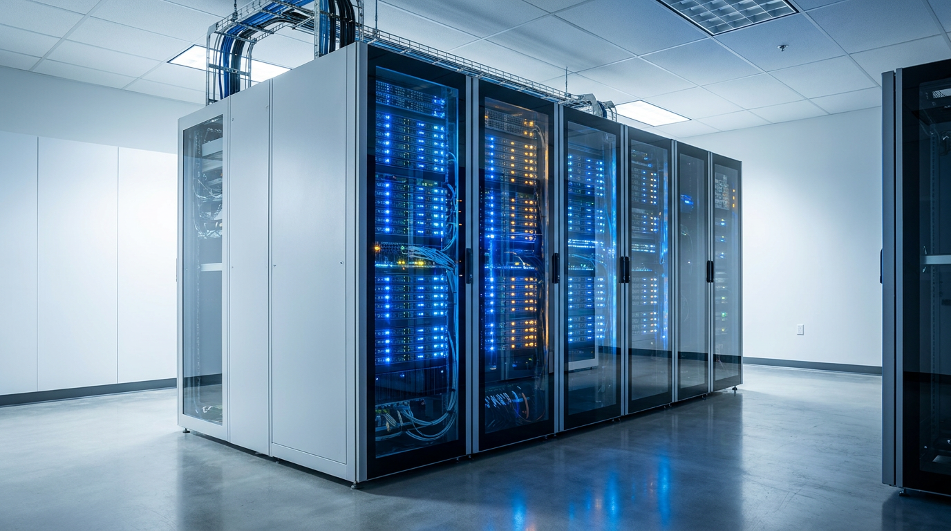
The artificial intelligence industry is colliding with the laws of physics. As frontier models scale to trillions of parameters, the data centers required to train them are drawing gigawatts of power, rivaling the energy consumption of small cities. Inside these massive facilities, traditional electronic graphics processing units (GPUs) are hitting a thermal and physical wall. Electrons traveling through copper wires face electrical resistance, generating massive amounts of heat and requiring extensive, energy-hungry cooling infrastructure.[5][6]
But the most pressing bottleneck isn't just computation—it is communication. In modern AI clusters, thousands of GPUs must constantly share data to train a single model. Copper interconnects simply cannot move information fast enough, leaving multi-million-dollar processors sitting idle while they wait for data to arrive. To solve this, the semiconductor industry is turning to a fundamentally different medium: light.[1][5]
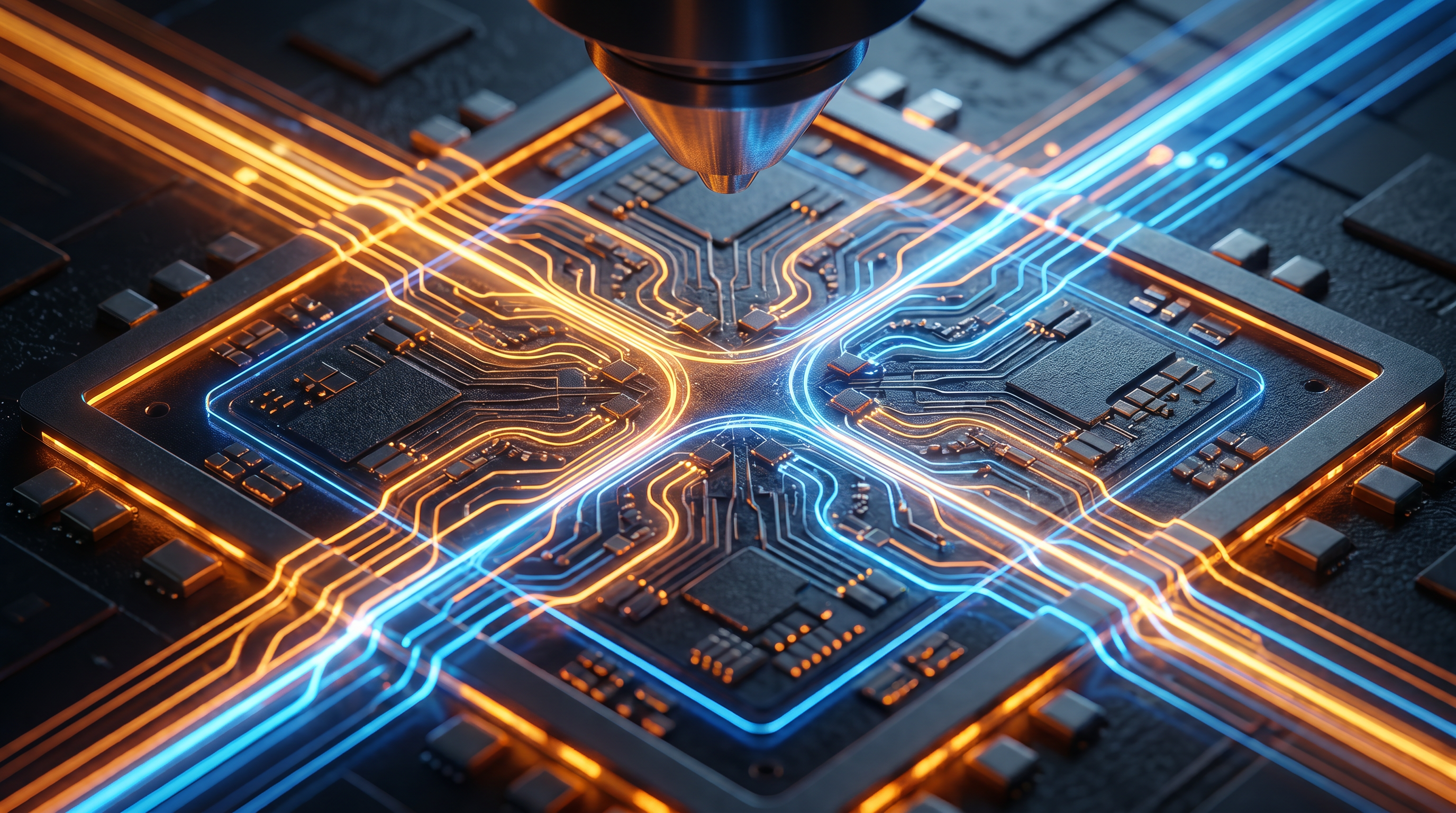
Silicon photonics is an emerging field that replaces electrical signals with optical ones. Instead of pushing electrons through copper, engineers are using photons—particles of light—to transmit and process data. Because photons travel without electrical resistance, they generate virtually no heat from data movement and can operate at the literal speed of light.[5]
The momentum behind this shift reached a critical tipping point in mid-2026. In June, silicon photonics startup Lightmatter announced it had joined NVIDIA's NVLink Fusion ecosystem, a major step toward integrating optical connectivity directly into dominant AI hardware architectures. By adapting bidirectional optical links, Lightmatter aims to reduce the massive fiber and connector requirements in AI data centers by 50 percent, simplifying the physical footprint of hyperscale clusters.[7]

The startup ecosystem is also accelerating rapidly. Paris-based Arago recently emerged from stealth with a $26 million seed round to build energy-efficient, light-based AI chips. The company claims its optical architecture can reduce energy consumption by 10 to 30 times compared to conventional NVIDIA GPUs, targeting enterprises looking to lower the exorbitant costs of running AI models.[4]
To understand why photonics offers such a massive leap, it helps to look at the microscopic architecture of these chips. A photonic integrated circuit relies on a few essential components. First, microscopic lasers generate the light. Second, silicon waveguides act as microscopic optical highways, steering the light across the chip.[5]
The actual computation happens in the third component: Mach-Zehnder Interferometers (MZIs). These microscopic structures split and recombine light waves. By altering the phase of the light as it passes through, MZIs can perform linear matrix multiplication—the fundamental mathematical operation that underpins all neural networks. Because this math is performed by the physical interference of light waves, it happens nearly instantaneously as the light passes through the chip.[5]
The actual computation happens in the third component: Mach-Zehnder Interferometers (MZIs).
Photonics also solves the bandwidth crisis through a technique called Wavelength Division Multiplexing (WDM). In traditional electronics, adding more bandwidth requires adding more physical copper wires. In optical systems, engineers can send multiple different colors (wavelengths) of light down the exact same waveguide simultaneously. Because the different colors do not interfere with one another, a single optical path can carry exponentially more data.[5]

While companies like Lightmatter are focused on using light to connect electronic GPUs, academic researchers are pushing the boundaries of using light for the actual AI processing. Researchers at the University of Florida recently developed a silicon photonic chip that achieved up to a 100-fold improvement in power efficiency while maintaining 98 percent accuracy in standard classification tasks.[8]
Similarly, Chinese research institutions have demonstrated all-optical computing chips that allegedly outperform conventional GPUs by massive margins in narrowly defined generative tasks. One such architecture, the Taichi-II chiplet developed at Tsinghua University, utilizes a "fully forward mode" that allows the AI to adjust its parameters instantly without multiple processing steps.[2][3]
The efficiency gains demonstrated in these lab environments are staggering. In low-light conditions, the Taichi-II chip reportedly achieved a million-fold improvement in energy efficiency compared to its predecessor, performing 160 trillion operations per watt. By comparison, most conventional electronic chips designed for similar tasks typically perform well under 10 trillion operations per watt.[3]

Taking inspiration from biology, some engineers are developing "neuromorphic" photonic systems. These architectures apply optical hardware to emulate the structure of the human brain, using spiking photonic neurons and optical synapses. Because neuromorphic systems process information in a massively parallel, asynchronous manner, they offer sub-nanosecond latency that is ideal for edge AI, robotics, and autonomous vehicles.[6]
Despite the immense promise, the transition to light is not without significant physical hurdles. The most fundamental challenge is size. Because the wavelength of light is physically larger than an electron, optical components cannot be miniaturized to the extreme nanometer scales of modern electronic transistors. This limits the overall packing density of photonic chips.[5]
Furthermore, the industry has yet to solve the optical memory bottleneck. While light is exceptional at moving and multiplying data, it is notoriously difficult to store. Current photonic systems must constantly convert optical signals back into electrical signals to store data in standard electronic memory banks, introducing latency and energy loss that undercuts the benefits of the optical processing.[5]

Because of these physical realities, experts agree that the near future of AI hardware is not entirely optical. Instead, the industry is moving toward hybrid co-packaged systems. In these architectures, traditional silicon electronics will continue to handle memory storage and logical control, while photonic circuits will be deployed specifically for heavy matrix multiplication and high-speed data transfer.[1][5]
As artificial intelligence continues its march toward trillion-parameter models and real-time video generation, the energy demands of the industry are becoming a global infrastructure challenge. Silicon photonics offers a viable off-ramp from this exponential power curve. By shifting the medium of computation from the electron to the photon, the semiconductor industry is laying the groundwork for AI systems that are not only vastly faster, but fundamentally more sustainable.[4][8]
How we got here
1960s-1980s
Early theoretical foundations of optical computing are established, though manufacturing limitations prevent practical application.
2017
Researchers demonstrate early on-chip neural networks based on silicon photonic technology, proving the concept of optical matrix multiplication.
2024
Tsinghua University unveils the Taichi chip architecture, demonstrating massive scalability for light-based artificial neural networks.
June 2026
Lightmatter joins the NVIDIA NVLink Fusion ecosystem, signaling the mainstream commercial integration of optical interconnects in AI data centers.
Viewpoints in depth
Commercial Photonics Innovators
Startups focused on solving immediate data center bottlenecks by replacing copper interconnects with optical links.
For commercial startups like Lightmatter and Arago, the immediate value of photonics lies in solving the data-movement crisis. Modern AI clusters are bottlenecked by the physical limitations of copper wires, which cannot move data fast enough to keep GPUs fully utilized. By replacing these electrical interconnects with optical links, these innovators argue they can drastically reduce training times and cut energy consumption by up to 30 times. Their focus is on building hybrid systems that can seamlessly integrate into existing electronic ecosystems, such as NVIDIA's NVLink, rather than trying to replace the entire computing stack overnight.
Academic Research Labs
Institutions pushing the boundaries of all-optical computing and neuromorphic designs for exponential efficiency gains.
Academic researchers at institutions like Tsinghua University and the University of Florida are looking past hybrid interconnects toward a future of all-optical processing. These labs argue that the true potential of photonics will only be unlocked when the actual matrix multiplication and neural network training happen entirely within the optical domain. By developing architectures like the Taichi-II chip and neuromorphic spiking networks, they have demonstrated theoretical efficiency gains of up to a million-fold. Their focus is on overcoming the fundamental physics challenges of optical memory and component miniaturization to build the foundation for artificial general intelligence hardware.
Hardware Ecosystem Integration
Analysts and engineers emphasizing that photonics must seamlessly integrate with existing electronic components and software.
Industry analysts and incumbent hardware engineers caution that photonics is not a standalone silver bullet. Because light is notoriously difficult to store, and optical components cannot be miniaturized to the same degree as electronic transistors, these experts argue that the future is inherently hybrid. They emphasize that the success of photonic chips depends entirely on 'co-packaged optics'—the ability to manufacture silicon chips that place optical transmitters side-by-side with traditional electronic memory and logic cores. For this camp, the software ecosystem and backward compatibility are just as important as the physical hardware breakthroughs.
What we don't know
- How quickly the semiconductor manufacturing supply chain can scale up production of hybrid electro-optical chips.
- Whether researchers can solve the optical memory bottleneck to allow for true all-optical computing without electronic conversion.
Key terms
- Silicon Photonics
- A technology that integrates optical components onto silicon chips, allowing data to be processed and transmitted using light.
- Mach-Zehnder Interferometer (MZI)
- A microscopic device on a photonic chip that splits and recombines light waves to perform mathematical calculations instantly.
- Wavelength Division Multiplexing (WDM)
- A technique that sends multiple different colors of light down the same path simultaneously to increase data bandwidth without adding wires.
- Neuromorphic Computing
- Hardware designed to mimic the physical structure and asynchronous processing style of the human brain's neural networks.
Frequently asked
Will photonic chips replace traditional GPUs entirely?
No. Experts predict a hybrid future where traditional electronics handle memory and logic, while photonics handle heavy math and data transfer.
Why are photonic chips more energy efficient?
Unlike electrons traveling through copper, photons (light) do not experience electrical resistance, meaning they generate virtually no heat when moving.
Can I buy a photonic AI computer today?
Not for personal use. The technology is currently being deployed at the enterprise level in massive AI data centers to connect servers and accelerate training.
What is the biggest challenge for photonic chips?
Storing light is notoriously difficult. Photonic systems still rely on electronic memory, creating a conversion bottleneck where light must be turned back into electricity to be stored.
Sources
Source coverage
8 outlets
3 viewpoints surfaced


[1]Network WorldCommercial Photonics Innovators
Lightmatter announces new silicon photonics products to tackle AI bottlenecks
Read on Network World →[2]TechRadarAcademic Research Labs
Chinese photonic chips reportedly outperform conventional GPUs in narrow, specialized generative AI tasks
Read on TechRadar →[3]Live ScienceAcademic Research Labs
Researchers Say Taichi-II Is a Major Leap Toward Scalable, Light-Based AI Systems
Read on Live Science →[4]SiftedCommercial Photonics Innovators
Nvidia challenger Arago raises $26m seed for light-based AI chips
Read on Sifted →[5]FindLightHardware Ecosystem Integration
Photonics for AI Hardware Acceleration
Read on FindLight →[6]arXivAcademic Research Labs
Neuromorphic Photonics and AI Computing
Read on arXiv →[7]Financial ContentCommercial Photonics Innovators
Lightmatter Joins NVIDIA NVLink Fusion and Powers Next-Generation AI Infrastructure with Photonic Interconnects
Read on Financial Content →[8]Artificial Intelligence NewsAcademic Research Labs
Revolutionary Light-Based AI Chip Achieves 100X Power Efficiency Breakthrough
Read on Artificial Intelligence News →
More in ai
See all 5 stories →On-Device AI
How Local AI Replaced the Cloud: Running Frontier Models on Your Laptop
0 sources

Enterprise AI
The Rise of Small Language Models: How Enterprises Are Running AI Locally in 2026
0 sources
Drug Discovery
New AI Model Accelerates Molecular Simulations 10,000-Fold, Slashing Drug Discovery Timelines
0 sources

Every angle. Every day.
Get ai stories with full source coverage and perspective breakdowns delivered to your inbox.