The Backside Power Delivery Revolution: How Flipping the Chip is Saving Moore's Law
As AI chips hit physical limits, semiconductor giants are moving power delivery to the back of the silicon wafer—a breakthrough that slashes energy loss and frees up critical space for data routing.
By Factlen Editorial Team
- Foundry Leaders
- The world's top chipmakers view backside power as the critical differentiator in the race for sub-2nm supremacy.
- AI Chip Designers
- Companies designing AI accelerators see backside power as a vital release valve for routing congestion.
- Manufacturing Equipment Suppliers
- The companies that build semiconductor fabrication tools view the transition as a massive new revenue cycle.
What's not represented
- · Data Center Operators
- · Thermal Management Engineers
Why this matters
AI data centers are consuming unprecedented amounts of electricity, threatening the sustainability of the AI boom. Backside power delivery dramatically improves energy efficiency and allows for denser, faster chips, ensuring the continued scaling of high-performance computing without melting down the grid.
Key points
- Traditional chips route both power and data through the front of the wafer, causing congestion and energy loss.
- Backside Power Delivery Networks (BSPDN) move the power infrastructure to the back of the chip.
- This separation reduces power loss by up to 30% and frees up space for denser data routing.
- Intel is launching its PowerVia technology in 2026, while TSMC follows with its Super Power Rail in Q3 2026.
The artificial intelligence boom is hitting a physical wall, and it is not just about the microscopic size of the transistors. It is about the microscopic traffic jam happening directly on top of them. As hyperscale data centers consume gigawatts of power to train next-generation generative models, the silicon chips themselves are beginning to choke on their own power supply infrastructure.
For decades, the global semiconductor industry has followed a standard, highly successful blueprint. Transistors are etched into the bottom of a silicon wafer, and a towering microscopic skyscraper of metal wiring is built on top of them. This "front-side" metal stack has historically been forced to do two highly demanding jobs simultaneously: deliver electricity to power the transistors, and route data signals between them.
But as transistors have shrunk to the scale of mere atoms, this dual-purpose highway has become hopelessly congested. Power lines and signal lines are fighting for the same increasingly scarce real estate. The result is a phenomenon known as "IR drop"—a severe loss of voltage as electricity travels through the labyrinth of microscopic wires, wasting energy as heat and artificially throttling the chip's maximum performance.
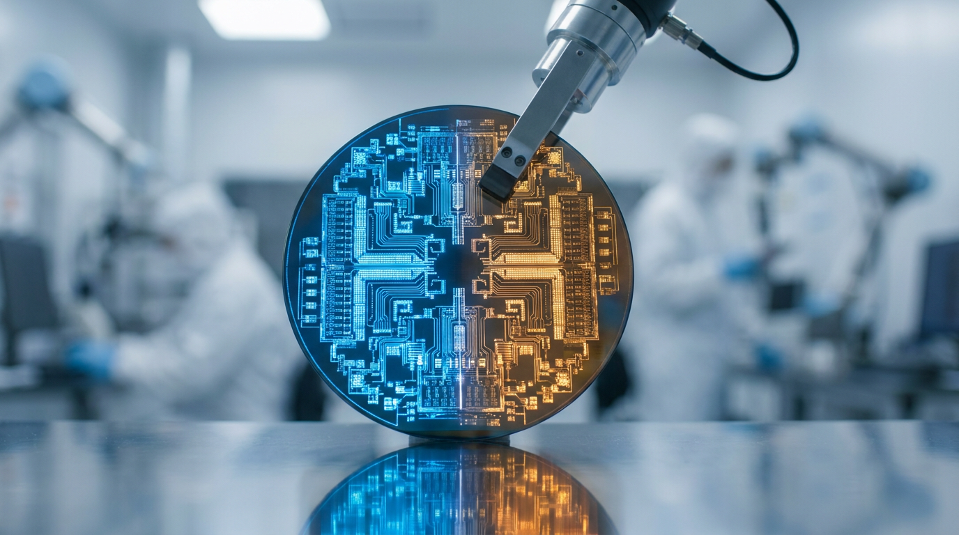
Enter the Backside Power Delivery Network (BSPDN), a fundamental architectural shift that is poised to save Moore's Law. Instead of forcing power and data to share the front-side metal stack, BSPDN physically separates them. The data signals stay on the front, while the entire power delivery infrastructure is moved to the back of the silicon wafer.[5]

"By removing power delivery resources from the front side, we open up additional routing resources on the front side, improving routability and area utilization," explains Dan Dechene, director of technology readiness at IBM Research. This decoupling allows chip designers to optimize each side of the silicon for its specific task, rather than compromising on both.[3][6]
The performance gains unlocked by this separation are staggering. According to industry benchmarking, moving power to the backside enables a 20% to 30% reduction in IR drop. It also allows for a 5% to 15% reduction in the core area of the chip, meaning significantly more transistors can be packed into the same physical footprint. In the high-stakes world of AI accelerators, these margins are the difference between leading the market and obsolescence.[6]
The transition is not a distant theoretical concept; it is happening right now. The three leading global foundries—TSMC, Intel, and Samsung—have all committed to introducing backside power delivery in their most advanced manufacturing nodes between 2026 and 2027. This architectural flip has become the immediate battleground for semiconductor supremacy.[4]

The transition is not a distant theoretical concept; it is happening right now.
Intel has been the most aggressive early mover with its proprietary implementation, dubbed "PowerVia." PowerVia is a cornerstone of the Intel 18A process node, which is currently ramping up for commercial production. The company's upcoming Core Ultra Series 3 client processors, code-named Panther Lake, will be among the first consumer products to feature the technology.[1][7]
Intel's approach relies on "nano-Through Silicon Vias" (nTSVs). These are microscopic vertical tunnels drilled completely through the silicon substrate, connecting the backside power grid directly to the transistor layer. It is a highly complex manufacturing feat, requiring the silicon wafer to be polished down to an almost impossibly thin layer before the backside wiring can be applied.[6][7]
TSMC, the world's largest contract chipmaker, is taking a different and arguably more ambitious route with its "Super Power Rail" (SPR) technology. Scheduled for mass production in the third quarter of 2026 with its A16 node, TSMC's implementation bypasses the via stack entirely.[2][7]
Instead of using nTSVs, TSMC's Super Power Rail makes direct contact with the transistor's source and drain. This direct-contact approach is significantly harder to manufacture, requiring extreme alignment tolerances. However, it eliminates the electrical resistance introduced by the via stack, resulting in an even lower power delivery impedance and higher overall efficiency.[7][8]
The explicit bifurcation of TSMC's roadmap into distinct AI and mobile tiers is the foundry formally acknowledging that it is serving two markets with fundamentally different binding constraints. For AI data centers, the primary constraint is watts per FLOP. Super Power Rail is custom-built to solve this exact bottleneck, allowing chips to draw massive amounts of power without melting.[8]
Implementing BSPDN requires a massive overhaul of the semiconductor manufacturing process. Traditionally, chips are built from the bottom up. With backside power, the wafer must be physically flipped over mid-production. The silicon substrate is ground down to a thickness of just a few micrometers—thinner than a human hair—before the backside power rails are deposited.[4][6]

This introduces severe mechanical and thermal challenges. The ultra-thin wafers are incredibly fragile and prone to warping. Furthermore, sandwiching the heat-generating transistors between two layers of dense metal wiring complicates thermal management. Foundries are relying on new ultra-flat glass carriers and advanced bonding techniques to keep the wafers stable during the backside processing.[4]
Despite these manufacturing hurdles, the industry has no choice but to push forward. The energy demands of generative AI models are growing exponentially, and traditional front-side power delivery has reached its absolute physical limits. Backside power delivery is the critical unlock that will allow the next generation of AI accelerators to scale efficiently.[5][8]
As the semiconductor industry enters the angstrom era, the focus has shifted from merely shrinking transistors to fundamentally reimagining how they are connected and powered. By flipping the chip, engineers have bought Moore's Law a new lease on life, ensuring that the hardware foundation of the AI revolution remains solid for the next decade.[8]
How we got here
2023
Intel publicly commits to implementing backside power delivery (PowerVia) in its future 18A node.
Early 2024
Major foundries finalize the architectural blueprints for separating power and signal routing at the sub-3nm scale.
Q1 2026
Intel unveils Core Ultra Series 3 (Panther Lake) processors, marking the commercial debut of PowerVia.
Q3 2026
TSMC is scheduled to begin mass production of its A16 node, featuring the direct-contact Super Power Rail technology.
2027
Next-generation AI accelerators utilizing BSPDN are expected to deploy in hyperscale data centers globally.
Viewpoints in depth
Foundry Leaders
The world's top chipmakers view backside power as the critical differentiator in the race for sub-2nm supremacy.
For TSMC, Intel, and Samsung, the transition to BSPDN is not just an engineering milestone; it is a high-stakes commercial battle. Intel is betting heavily that its early adoption of PowerVia in the 18A node will allow it to reclaim process leadership. TSMC, meanwhile, is positioning its Super Power Rail as the premium solution for hyperscale AI customers who are willing to pay for maximum efficiency. The foundries recognize that whoever achieves the highest manufacturing yield with this complex "wafer-flipping" process will dominate the next decade of high-margin AI silicon contracts.
AI Chip Designers
Companies designing AI accelerators see backside power as a vital release valve for routing congestion.
Architects at companies like Nvidia, AMD, and IBM have been fighting a losing battle against front-side metal congestion. As they pack more transistors into their designs to handle massive AI models, the wiring required to connect them has become a labyrinthine bottleneck. By offloading the power delivery network to the backside, designers suddenly have access to a pristine, uncrowded front-side metal stack. This allows them to route data signals more efficiently, increasing memory bandwidth and overall computational throughput without increasing the physical size of the die.
Manufacturing Equipment Suppliers
The companies that build semiconductor fabrication tools view the transition as a massive new revenue cycle.
The shift to backside power delivery requires an entirely new suite of manufacturing equipment. Toolmakers like ASML, Applied Materials, and Lam Research are developing specialized machines capable of grinding silicon wafers down to single-digit micrometer thicknesses without shattering them. They are also pioneering new metrology tools that can align the backside power grid with the front-side transistors using infrared light, achieving precision at the nanometer scale. For these suppliers, BSPDN represents a lucrative new frontier in the fabrication process.
What we don't know
- Yield rates at scale: While early prototypes are successful, it remains unclear how high defect rates will be when foundries attempt to mass-produce these ultra-thin, double-sided wafers.
- Long-term thermal reliability: Sandwiching heat-generating transistors between two dense layers of metal wiring presents novel cooling challenges that have yet to be tested over years of continuous data center operation.
- The cost premium: The additional manufacturing steps required to flip and thin the wafer will increase production costs, but the exact price premium for BSPDN chips is still unknown.
Key terms
- BSPDN (Backside Power Delivery Network)
- An architecture that routes electrical power to transistors from the back of the silicon wafer, separating it from data signals.
- IR Drop
- The loss of electrical voltage that occurs as current travels through the resistance of microscopic metal wiring in a chip, wasting energy as heat.
- Node
- A specific generation of semiconductor manufacturing technology, often denoted by a nanometer or angstrom measurement (e.g., TSMC A16, Intel 18A).
- nTSV (nano-Through Silicon Via)
- Microscopic vertical tunnels drilled through silicon to connect different layers of a chip.
- PPA (Performance, Power, Area)
- The three primary metrics used by engineers to evaluate the quality and efficiency of a semiconductor design.
Frequently asked
What exactly is Backside Power Delivery?
It is a new chip architecture that routes electrical power to the transistors from the bottom (back) of the silicon wafer, rather than mixing power and data wires together on the top (front).
Why is this necessary for AI?
AI chips require massive amounts of electricity. Traditional designs cram power and data wires together, causing severe congestion and energy loss. Separating them allows chips to run faster and cooler.
What is the difference between Intel and TSMC's approach?
Intel uses microscopic vias (tunnels) to connect the back power grid to the transistors. TSMC's upcoming Super Power Rail connects directly to the transistor components, which is harder to manufacture but highly efficient.
When will these chips be available?
Intel is rolling out its PowerVia technology in consumer processors in 2026, while TSMC plans to mass-produce its A16 node with backside power in the second half of 2026.
Sources
Source coverage
8 outlets
3 viewpoints surfaced


[1]Intel NewsroomFoundry Leaders
Intel Achieves Breakthrough in Backside Power Delivery with PowerVia
Read on Intel Newsroom →[2]TSMC Press CenterFoundry Leaders
TSMC Unveils A16 Technology with Super Power Rail
Read on TSMC Press Center →[3]IBM ResearchAI Chip Designers
The future of chip scaling: Backside power delivery
Read on IBM Research →[4]Mitsui Global Strategic Studies InstituteManufacturing Equipment Suppliers
Backside Power Delivery: A Breakthrough in Semiconductor Scaling
Read on Mitsui Global Strategic Studies Institute →[5]PatSnap InsightsAI Chip Designers
Decoupling Power from Signal: The BSPDN Architecture
Read on PatSnap Insights →[6]Semiconductor EngineeringManufacturing Equipment Suppliers
Core Issues For Backside Power
Read on Semiconductor Engineering →[7]FiisualFoundry Leaders
TSMC's Backside Power Delivery Network and the A16 Process
Read on Fiisual →[8]Factlen Editorial TeamManufacturing Equipment Suppliers
Synthesis by Factlen editorial team
Read on Factlen Editorial Team →

Every angle. Every day.
Get technology stories with full source coverage and perspective breakdowns delivered to your inbox.