
Sony and TSMC Commit $6.3 Billion to Jointly Manufacture Next-Generation Image Sensors
Sony and TSMC are forming a $6.3 billion joint venture in Japan to mass-produce advanced image sensors for smartphones and physical AI applications.
By Tiago Sousa

If you are budgeting for a premium smartphone, a mirrorless camera, or a vehicle with advanced driver assistance in the coming years, the hardware dictating that purchase is shifting. The image sensor is no longer just a component that captures light; it is the primary processing engine for how devices interpret the physical world. Understanding who makes these sensors—and how they are built—is critical to knowing which tech ecosystem to invest in.
To dominate that future, Sony Group and Taiwan Semiconductor Manufacturing Co. (TSMC) are committing roughly $6.3 billion (1 trillion yen) to a new joint venture. The partnership will develop and mass-produce next-generation image sensors at a dedicated facility in Kumamoto, Japan.[1][3]
Under the reported terms, Sony will hold a 60% controlling stake, with TSMC owning the remaining 40%. The new entity, Advanced Vision Semiconductor Manufacturing Corporation, is expected to be formally established by March 2027, with commercial mass production slated to begin in 2029.[1][3][6]
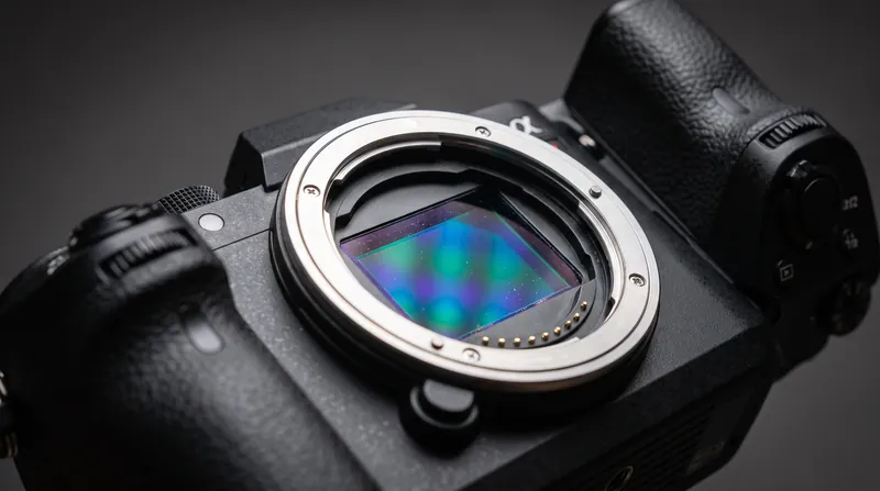
For buyers evaluating camera specs, the importance of this deal lies in how modern CMOS image sensors are constructed. High-end sensors rely on a "stacked" architecture, physically bonding a top pixel layer that captures light to a bottom logic layer that processes the digital signal.[4]
Historically, Sony designed the complete sensor and manufactured the pixel layer, but outsourced the complex logic layer to foundries like TSMC. As computational photography demands more processing power directly on the sensor, that arms-length contractor relationship is no longer efficient.[4][5]
By forming a joint venture, Sony integrates TSMC's advanced manufacturing and 3DFabric packaging technology directly into the research and development phase. This allows the two companies to co-design the silicon from the ground up, accelerating the timeline for bringing faster, more capable sensors to the consumer market.[5][6]
While the initial production lines will supply flagship smartphones—most notably Apple's future iPhones—the venture's long-term target is a category known as physical AI.[1][2][5]
Physical AI encompasses systems that interact autonomously with the real world, such as self-driving cars, delivery drones, and industrial robotics. These applications require sensors that can instantly process depth, motion, and object recognition without waiting for a central computer to interpret the data.[2][3]
Sony currently controls more than half of the global CMOS image sensor market. However, the landscape is tightening. Competitors like Samsung Electronics and China's OmniVision are aggressively expanding their own sensor manufacturing capabilities to capture the automotive and AI sectors.[2][4]
The $6.3 billion partnership serves as a defensive moat. It significantly reduces Sony's capital expenditure burden by splitting the costs of a new fabrication plant, while guaranteeing TSMC a steady stream of high-volume orders amid fluctuating global chip demand.[1][4]
The Kumamoto location also reshapes the consumer electronics supply chain. By anchoring this massive production hub in Japan, the venture insulates critical camera components from broader geopolitical trade tensions affecting other parts of Asia.[5]
The Japanese government views this domestic production as a national security priority. Sony and TSMC are actively negotiating with Japan's Ministry of Economy, Trade and Industry to secure substantial subsidies, ensuring the facility remains cost-competitive.[1][2]
For consumers, the takeaway is clear: the era of comparing cameras purely by megapixel count is over. The defining metric for future imaging gear will be how much AI processing power is embedded directly into the sensor itself.[2]
When this facility comes online in 2029, the resulting hardware will dictate the performance ceiling for the next decade of consumer electronics. By locking in TSMC's manufacturing dominance, Sony is positioning itself to remain the default choice for anyone buying high-end imaging technology.[2][6]
Viewpoints in depth
Joint Venture Partners
Sony and TSMC argue that deep integration is necessary to build the next generation of AI-capable sensors.
For Sony and TSMC, the traditional contractor relationship—where one company designs a chip and simply hands the blueprints to a factory—is no longer sufficient for high-end imaging. As sensors move toward advanced nodes and require complex 3DFabric stacking technology, the two companies argue that they must co-design the silicon from the ground up. By pooling their core R&D resources into a single entity, they aim to accelerate the commercialization of sensors built specifically for physical AI and automotive applications.
Industry Analysts
Market observers view the $6.3 billion deal as a defensive, risk-reducing maneuver.
Financial and semiconductor analysts see the Kumamoto joint venture as a highly pragmatic move to protect market share. Sony currently dominates the image sensor market but faces massive capital expenditure requirements to stay ahead of aggressive investments from Samsung and OmniVision. By splitting the $6.3 billion cost with TSMC, Sony significantly reduces its financial burden. Conversely, TSMC secures a guaranteed, high-volume customer for its advanced logic layers, insulating the foundry from broader fluctuations in the global chip market.
Imaging Enthusiasts
Camera and smartphone consumers are focused on the shift from megapixels to computational processing.
For the consumer electronics sector, the partnership signals a definitive end to the traditional megapixel race. Enthusiasts and tech reviewers note that the bottleneck in modern photography is no longer capturing light, but processing it instantly. By embedding TSMC's advanced logic directly into Sony's sensors, future devices will be able to perform complex AI tasks—like real-time object tracking and depth mapping—directly on the sensor, fundamentally changing the performance ceiling of flagship smartphones and mirrorless cameras.
Key points
- Sony and TSMC are forming a $6.3 billion joint venture to mass-produce next-generation image sensors in Japan.
- Sony will hold a 60% controlling stake, with TSMC owning the remaining 40%.
- The partnership integrates TSMC's advanced logic manufacturing directly with Sony's pixel design.
- Production will target flagship smartphones as well as physical AI applications like robotics and autonomous vehicles.
What we don’t know
- The exact amount of government subsidies Japan's Ministry of Economy, Trade and Industry will provide to the venture.
- How competitors like Samsung and OmniVision will adjust their capital expenditures in response to the Sony-TSMC alliance.
How we got here
May 2026
Sony and TSMC sign a non-binding memorandum of understanding to establish a strategic partnership for next-generation image sensors.
August 2026
Reports emerge detailing a $6.3 billion joint venture, with Sony holding a 60% stake and TSMC 40%.
March 2027
The targeted deadline for the formal establishment of the Advanced Vision Semiconductor Manufacturing Corporation.
2029
Expected commencement of commercial mass production at the Kumamoto facility.
- Joint Venture Partners
- Sony and TSMC argue that deep integration is necessary to build the next generation of AI-capable sensors.
- Industry Analysts
- Market observers view the $6.3 billion deal as a defensive, risk-reducing maneuver.
- Imaging Enthusiasts
- Camera and smartphone consumers are focused on the shift from megapixels to computational processing.
Perspectives this story doesn't cover
- Competitor Foundries (Samsung)
- Automotive Manufacturers
Sources
Source coverage
6 outlets
3 viewpoints surfaced






- [1]Investing.comIndustry Analysts
Sony, TSMC plan $6.3 billion JV to make image sensors in Japan, Nikkei reports
Read on Investing.com → - [2]Imaging ResourceImaging Enthusiasts
Sony and TSMC Team Up to Develop Next-Generation Image Sensors
Read on Imaging Resource → - [3]AnySiliconIndustry Analysts
Sony and TSMC Reportedly Plan $6.3 Billion Joint Venture for Next-Generation Image Sensors
Read on AnySilicon → - [4]Light ReadingIndustry Analysts
TSMC and Sony to form $4.69 billion chip venture in Japan
Read on Light Reading → - [5]AI WeeklyIndustry Analysts
Sony and TSMC set $6.3B Kumamoto JV for next-gen image sensors
Read on AI Weekly → - [6]TSMCJoint Venture Partners
Sony Semiconductor Solutions and TSMC Announce Joint Venture
Read on TSMC →
More in Shopping & Reviews
See all →Chroma Subsampling
4:2:2 vs. 4:2:0 Chroma Subsampling: How Two Numbers Dictate Video Color Grading Flexibility
6 sources
Camera Tech
Phase Detection vs. Contrast Detection Autofocus: How On-Sensor Microlenses Dictate Speed and Accuracy
8 sources
Image Stabilization
Optical Lens Stabilization and Sensor-Shift Systems: How Camera Shake Correction Dictates Low-Light Performance
7 sources
Sensor Physics
The Physics of Camera Sensors: Comparing Full-Frame, APS-C, and Micro Four Thirds
3 sources
Comments
Every angle. Every day.
Get Shopping & Reviews stories with full source coverage and perspective breakdowns, free every day.