How Photonic Chips Are Rewiring AI to Run on Light
As traditional GPUs hit physical and thermal limits, a new generation of photonic accelerators is using light to process AI workloads, promising massive leaps in speed and energy efficiency.
By Factlen Editorial Team
- Optical Hardware Innovators
- Startups and researchers pushing to replace electronic bottlenecks with light-speed optical computing.
- Incumbent Chipmakers
- Traditional semiconductor giants integrating photonics for data transfer while keeping computation electronic.
- Skeptical Analysts
- Industry observers who note that optical computing is currently limited to narrow, specialized tasks rather than general-purpose AI.
What's not represented
- · Environmental advocates assessing the actual carbon-reduction impact of optical data centers.
- · Software engineers tasked with rewriting AI frameworks to compile code for analog optical hardware.
Why this matters
The exponential growth of artificial intelligence is currently constrained by the massive electricity demands and heat output of traditional silicon chips. Transitioning to light-based computation could slash data center energy consumption by up to 90%, making advanced AI both economically and environmentally sustainable.
Key points
- Photonic AI chips use light (photons) instead of electricity to perform the matrix multiplications required for neural networks.
- Because light encounters no electrical resistance, optical chips generate virtually no heat and consume vastly less energy.
- Wavelength Division Multiplexing allows multiple data streams to be processed simultaneously using different colors of light.
- Major foundries like TSMC have begun mass-producing silicon photonics platforms, enabling commercial deployment in 2026.
- While highly efficient for specific tasks, optical chips currently serve as specialized accelerators rather than full replacements for general-purpose GPUs.
The artificial intelligence boom is colliding with the laws of physics. As large language models scale into the trillions of parameters, the traditional electronic hardware used to train and run them—primarily Graphics Processing Units (GPUs)—is hitting a severe "power wall."[1][6]
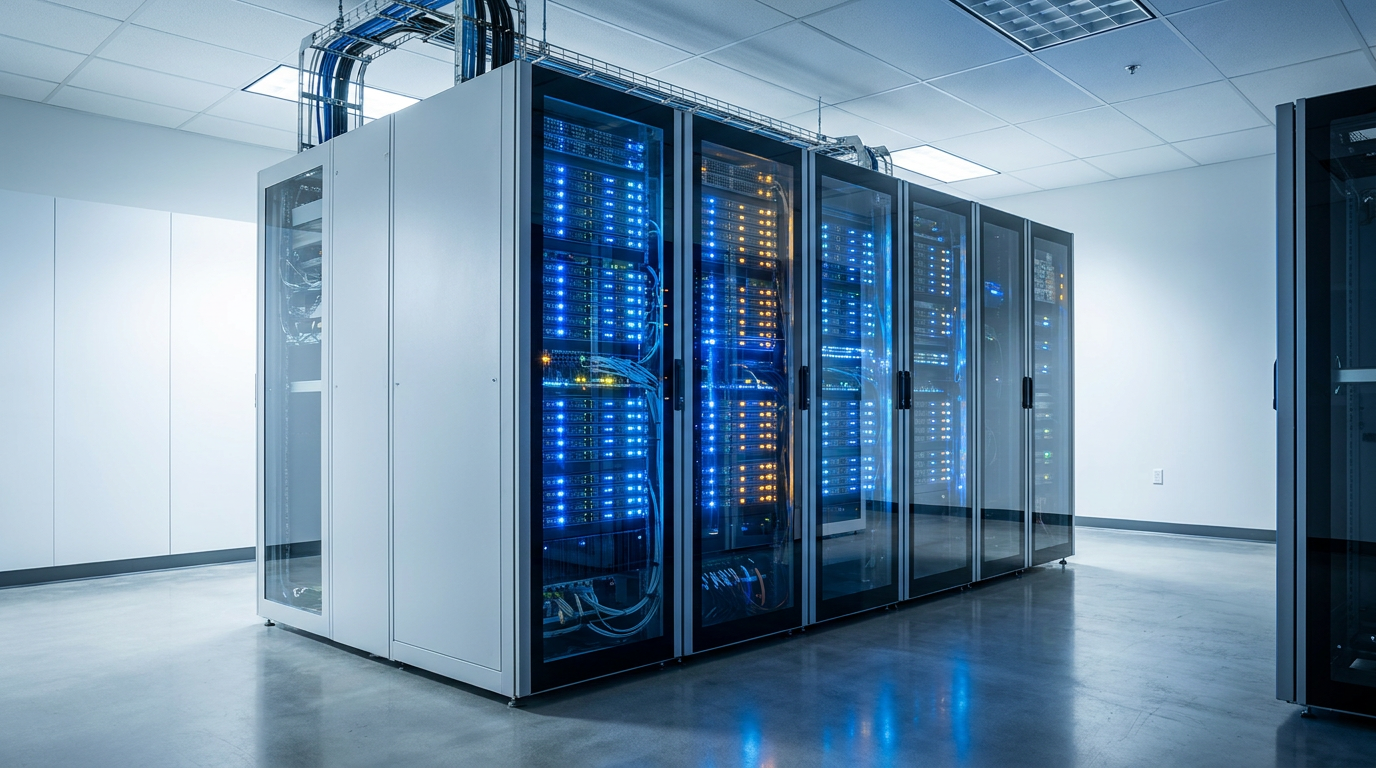
Modern AI data centers now consume terawatt-hours of electricity annually, generating immense heat that requires massive, energy-intensive cooling infrastructure. Furthermore, pushing electrons through silicon and copper interconnects creates physical resistance, slowing down data transfer and capping the ultimate performance of the hardware.[6][7]
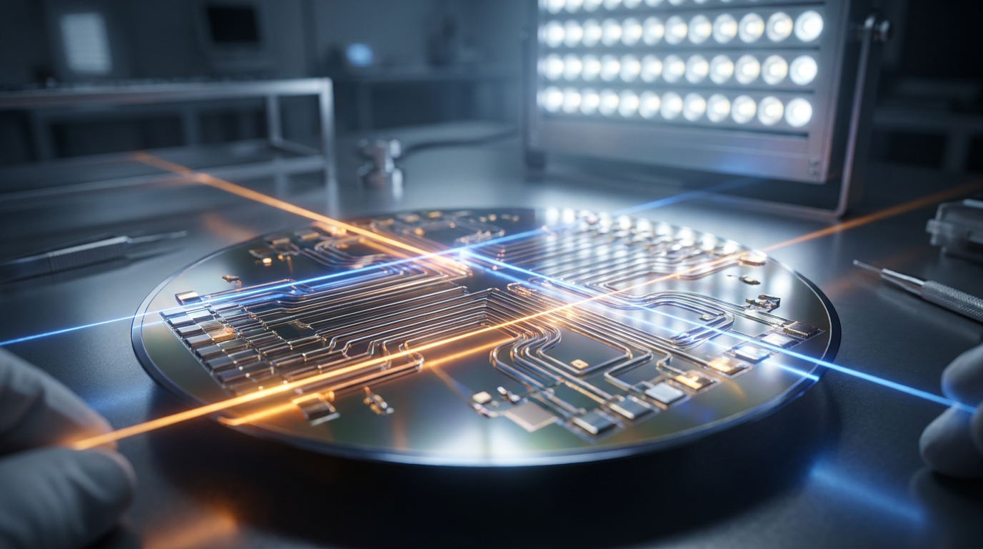
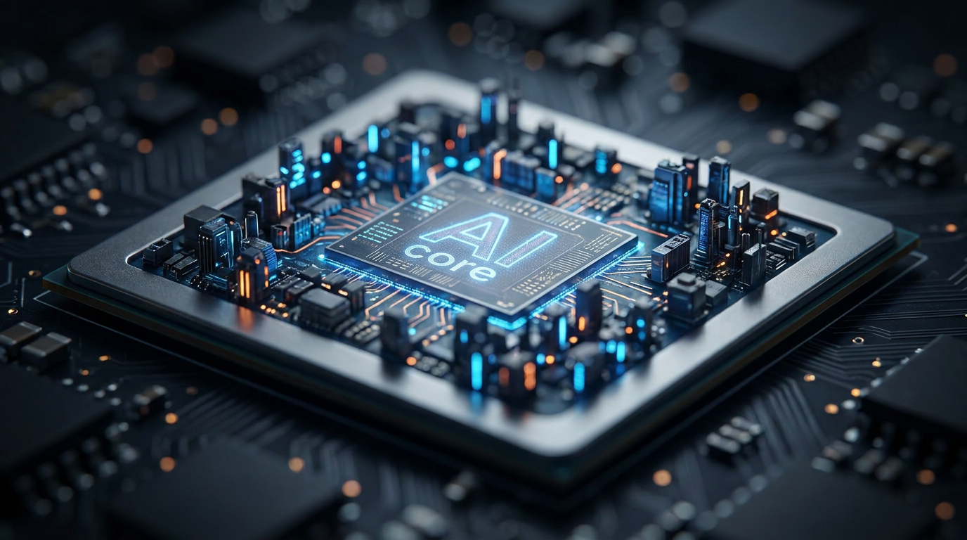
To break this bottleneck, the semiconductor industry is turning to a radically different substrate: light. Photonic AI accelerators, which use photons instead of electrons to perform computations, are rapidly moving from laboratory prototypes to commercial production, promising a paradigm shift in how machines process information.[1][2]
By leveraging the principles of optical physics, these specialized chips can execute the core mathematical operations of neural networks at the speed of light, all while consuming a mere fraction of the energy required by traditional silicon processors.[2][3]

At the heart of this shift is a fundamental change in how data is represented and manipulated. In a conventional GPU, billions of microscopic transistors act as physical switches, turning electrical currents on and off to represent binary data and perform logic operations.[4]
Photonic chips, by contrast, feed data into the system using microscopic lasers that emit light pulses into silicon waveguides. These waveguides act as tiny optical roads built directly into the chip, guiding the light through a maze of computational components without relying on electrical wires.[7]
The actual computation relies on intricate structures called Mach-Zehnder Interferometers (MZIs). Instead of switching electrons on and off, MZIs split a beam of light into two separate paths, alter the phase of the light, and then recombine the waves.[7]
When these light waves interfere with one another upon recombining, their combined amplitudes naturally perform matrix multiplication—the dense linear algebra that serves as the mathematical backbone of all deep learning models. Because this happens optically, the calculation is performed almost instantaneously as the light passes through the chip.[4][6][7]

Because this happens optically, the calculation is performed almost instantaneously as the light passes through the chip.
One of the most powerful advantages of optical computing is its capacity for massive parallelism, enabled by a technique known as Wavelength Division Multiplexing (WDM).[7]
Unlike electrical signals, which can interfere with each other if sent down the same copper wire simultaneously, different colors (wavelengths) of light can travel through the exact same optical waveguide at the exact same time without mixing. This allows a single photonic chip to process thousands of data streams concurrently, dramatically increasing overall throughput.[7]
The energy savings associated with this method are equally profound. Because photons do not experience electrical resistance as they travel, they generate virtually no heat as they move through the optical circuits.[3][7]
Leading photonic AI systems can perform inference tasks using roughly 1 to 10 femtojoules per operation. By comparison, state-of-the-art electronic GPUs consume between 50 and 500 picojoules per operation—meaning optical computing can be up to 50 to 500 times more energy-efficient for specific AI workloads.[6]
The commercial ecosystem for this technology matured rapidly in early 2026. In April, Taiwan Semiconductor Manufacturing Company (TSMC) pushed its COUPE silicon photonics platform into mass production, a watershed moment that makes co-packaged optics available beyond a few hyperscale tech giants.[1]
Startups are aggressively capitalizing on this manufacturing readiness. Ayar Labs recently closed a $500 million Series E funding round to scale volume production of its TeraPHY optical engine chiplets, which use light to move data between AI accelerators at unprecedented speeds, eliminating the traditional copper bottleneck.[1]

Similarly, Lightmatter is integrating its Passage optical interconnect technology directly with customer chip designs to network massive GPU clusters. Meanwhile, in Europe, Q.ANT recently launched a dedicated €14 million production line in Stuttgart to manufacture specialized photonic chips using thin-film lithium niobate, a material that allows for ultra-fast optical signal manipulation.[1][3]
Despite these breakthroughs, optical computing is not yet a wholesale replacement for general-purpose GPUs. Photonic chips currently excel at narrow, specialized generative AI tasks and specific matrix multiplications, but they lack the flexible programmability of traditional electronic circuits.[4]
Furthermore, the analog nature of light means that achieving the exact computational precision required for some AI training workloads remains a challenge. As a result, the most effective near-term architectures are hybrid systems that pair optical compute cores with traditional electronic controllers.[4][7]
Nevertheless, as the industry standardizes around co-packaged optics and photonic interconnects, the line between optical communication and optical computation is blurring. With AI's energy demands threatening to outstrip global grid capacity, the transition to light-speed computing is rapidly becoming an infrastructural necessity.[3][5][6]
How we got here
2018-2020
Early academic research demonstrates the viability of using Mach-Zehnder Interferometers for neural network computation.
2024
Lightmatter raises a $400M Series D, signaling major venture capital confidence in commercializing optical compute.
Feb 2025
Q.ANT launches a dedicated production line in Germany for thin-film lithium niobate photonic chips.
Mar 2026
Ayar Labs secures $500M to scale volume production of its TeraPHY optical engine chiplets.
Apr 2026
TSMC's COUPE silicon photonics platform enters mass production, opening the door for widespread co-packaged optics.
Viewpoints in depth
Silicon Photonics Startups
Companies building optical chips argue that light is the only physical way to scale AI sustainably.
Startups like Lightmatter and Ayar Labs view the current electronic 'power wall' as an insurmountable physics problem for traditional copper and silicon. They argue that as AI models grow to trillions of parameters, the energy required simply to move data between chips will bankrupt data centers. By transitioning to optical interconnects and photonic compute cores, they believe the industry can achieve 100x improvements in energy efficiency while drastically reducing latency.
Traditional GPU Manufacturers
Incumbent chipmakers view photonics as a complementary technology rather than a total replacement.
While companies like Nvidia are heavily investing in optical networking to connect their server racks, they maintain that general-purpose electronic GPUs will remain the workhorses of AI for the foreseeable future. They point out that optical computing struggles with the flexible programmability and high-precision floating-point math required for end-to-end model training. In their view, photonics will handle data transmission and specific inference tasks, while electrons will continue to handle the core logic.
Hyperscale Cloud Providers
Major tech giants are urgently seeking optical solutions to manage their skyrocketing energy footprints.
For operators of massive data centers, the appeal of photonics is strictly operational and environmental. Facing regulatory pressure over their massive electricity consumption and struggling to secure enough power for new facilities, hyperscalers see co-packaged optics and photonic accelerators as a critical lifeline. Their primary focus is on reducing the total cost of ownership (TCO) and cooling requirements, making them eager early adopters of any technology that lowers the energy-per-operation metric.
What we don't know
- Whether photonic chips can achieve the high-precision floating-point accuracy required to train the largest foundational AI models from scratch.
- How quickly the software ecosystem and AI frameworks (like PyTorch) will adapt to natively support optical hardware architectures.
- Which startup's specific optical interconnect standard will ultimately be adopted by the broader semiconductor industry.
Key terms
- Silicon Photonics
- The study and application of photonic systems that use silicon as an optical medium, allowing light-based components to be manufactured using traditional chip-making facilities.
- Mach-Zehnder Interferometer (MZI)
- An optical device that splits a beam of light into two paths and recombines them; the resulting interference is used to perform mathematical calculations.
- Wavelength Division Multiplexing (WDM)
- A technology that multiplexes a number of optical carrier signals onto a single optical fiber by using different wavelengths (colors) of laser light.
- Co-Packaged Optics (CPO)
- An advanced manufacturing technique that integrates optical transceivers directly into the same package as the main processor, drastically reducing power consumption.
- Femtojoule
- A unit of energy equal to one quadrillionth of a joule, used to measure the extreme energy efficiency of optical computing operations.
Frequently asked
Will photonic chips replace my computer's CPU or GPU?
Not in the near future. Photonic chips are currently designed as specialized accelerators for data centers to handle massive AI workloads, rather than general-purpose processors for personal computers.
Why are photonic chips more energy-efficient?
Unlike electrons traveling through copper wires, photons do not experience electrical resistance. This means they can transmit and process data without generating the massive amounts of heat that plague traditional silicon chips.
Can optical chips train AI models?
While they excel at AI inference (running already-trained models), training models from scratch requires high-precision math that is currently difficult to achieve with the analog nature of light. Most training still relies on electronic GPUs.
Sources
Source coverage
7 outlets
3 viewpoints surfaced


[1]Next Waves InsightOptical Hardware Innovators
Photonic Compute Hits Production: Lightmatter, Ayar Labs, and Co-Packaged Optics Are Now Shipping
Read on Next Waves Insight →[2]SciTechDailyOptical Hardware Innovators
A Leap Forward: Photonic Circuits for AI
Read on SciTechDaily →[3]The Brighter Side of NewsOptical Hardware Innovators
Revolutionary photonic AI chips are set to dramatically boost computing speed, efficiency, and sustainability worldwide
Read on The Brighter Side of News →[4]TechRadarSkeptical Analysts
Chinese photonic chips reportedly outperform conventional GPUs in narrow, specialized generative AI tasks
Read on TechRadar →[5]Yole GroupIncumbent Chipmakers
Silicon Photonics 2025 and Co-Packaged Optics for Data Centers 2025
Read on Yole Group →[6]DataInteloIncumbent Chipmakers
Photonic AI Accelerator Chip Market Outlook 2025-2034
Read on DataIntelo →[7]MediumSkeptical Analysts
System Architecture of a Photonic AI Processor
Read on Medium →
More in ai
See all 5 stories →On-Device AI
How Local AI Replaced the Cloud: Running Frontier Models on Your Laptop
0 sources

Enterprise AI
The Rise of Small Language Models: How Enterprises Are Running AI Locally in 2026
0 sources
Drug Discovery
New AI Model Accelerates Molecular Simulations 10,000-Fold, Slashing Drug Discovery Timelines
0 sources

Every angle. Every day.
Get ai stories with full source coverage and perspective breakdowns delivered to your inbox.