
How IBM's 0.7-Nanometer 'Nanostack' Chip Breaks the Physical Limits of Silicon
By stacking transistors vertically, IBM has unveiled the world's first sub-1 nanometer chip architecture, promising a 70% reduction in energy use that could reshape the future of AI infrastructure.

Share this story
For more than six decades, the semiconductor industry has operated under a simple, relentless mandate: shrink the transistor, pack more of them onto a flat piece of silicon, and reap the rewards of faster, cheaper computing. But in recent years, that lateral shrinkage has collided with the laws of physics. As transistor gates approach the width of a few dozen atoms, quantum tunneling and heat dissipation make further two-dimensional scaling nearly impossible.
On Thursday, IBM announced a breakthrough that effectively bypasses this physical wall. The company unveiled the world's first sub-1 nanometer chip technology, operating at the 0.7-nanometer—or 7 angstrom—node. By moving away from a flat plane and building upward into the Z-axis, IBM has managed to cram nearly 100 billion transistors onto a piece of silicon roughly the size of a fingernail.
The implications for the computing industry, particularly the energy-starved artificial intelligence sector, are massive. According to IBM's technical data, the new architecture can deliver either a 50 percent increase in raw performance or a 70 percent reduction in energy consumption compared to the 2-nanometer chips the company introduced in 2021.[1]
To understand how this works, it helps to look at the evolution of transistor design. For years, the industry relied on FinFET (Fin Field-Effect Transistor) technology, which used a 3D fin-like structure to control electrical current. When FinFET reached its limits, IBM pioneered the "nanosheet" in 2017—a gate-all-around design where the transistor channel consists of horizontal silicon ribbons completely surrounded by a gate, preventing electrical leakage. Nanosheets are now the standard for the current generation of 3nm and 2nm chips.[1][2]
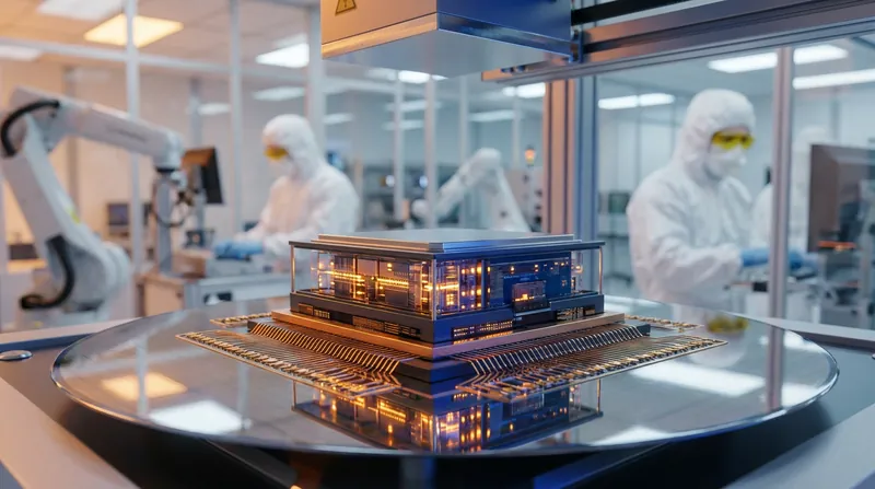
IBM's new breakthrough, dubbed the "nanostack," takes the nanosheet and adds a third dimension. Instead of placing the two fundamental types of transistors—n-type (NFET) and p-type (PFET)—side by side on a wafer, the nanostack architecture literally stacks them on top of each other.[2]
"With our new nanostack architecture, we're not just making smaller transistors, we're reinventing how chips are built," said Jay Gambetta, Director of IBM Research. He noted that the design allows the industry to continue scaling for at least another decade without running afoul of atomic limits.[1]
The manufacturing process required to achieve this vertical stacking is extraordinarily complex. The two transistors are built on separate wafers and then joined using a technique called ultra-thin dielectric bonding. The bonding oxide layer that separates them is kept below 30 nanometers to minimize electrical capacitance penalties.
Crucially, this vertical separation allows engineers to use different, optimized materials for the top and bottom layers. Because the NFET and PFET are fabricated independently before being bonded, each can be tuned for maximum performance or power efficiency without compromising the other.[2]
Furthermore, IBM's specific offset positioning of the upper-layer transistors reduces the complexity of the microscopic wiring—known as interconnects—that links the billions of switches together. This offset design solves a major bottleneck that has plagued other experimental 3D transistor efforts.[2]
The most immediate beneficiary of this architecture will be the artificial intelligence industry. Generative AI models require vast amounts of memory bandwidth, which is currently a binding constraint for data centers. IBM researchers demonstrated that the nanostack architecture enables a 40 percent scaling improvement in SRAM (Static Random-Access Memory), directly addressing the memory bottleneck that throttles AI workloads.
Beyond speed, the 70 percent energy efficiency gain offers a lifeline to an industry facing an infrastructure crisis. AI data centers are currently straining regional power grids and consuming millions of gallons of water for cooling. A chip that can perform the same trillions of operations per second while drawing less than a third of the power fundamentally alters the math of AI scaling.
However, a laboratory breakthrough is not a commercial product. The 0.7-nanometer chip is currently a research achievement developed at IBM's Albany Nanotech Complex in New York, in collaboration with equipment manufacturers like Lam Research and Tokyo Electron. IBM estimates it will take roughly five years for the technology to reach commercial production.[1][2]
The transition from the lab to the fab will require mastering High-NA EUV (Extreme Ultraviolet) lithography, the cutting-edge, $350 million machines built by ASML that are required to print circuits at the angstrom scale. Yield rates—the percentage of chips on a wafer that function correctly—will be the ultimate test of the nanostack's viability.[1]
Because IBM no longer manufactures its own chips, it will rely on foundry partners to bring the nanostack to market. While the company has not formally announced which foundries will license the 0.7nm technology, it is currently working closely with the Japanese state-backed startup Rapidus to commercialize its previous 2nm nanosheet designs.[1]
If successful, the nanostack architecture proves that the death of Moore's Law has been greatly exaggerated. By looking up instead of out, semiconductor engineers have found a new frontier in the Z-axis, ensuring that the foundational hardware of the digital age still has room to grow.
Key points
- IBM has unveiled the world's first sub-1 nanometer chip, operating at the 0.7nm (7 angstrom) node.
- The new 'nanostack' architecture stacks transistors vertically, doubling density compared to 2nm chips.
- The design promises up to 50% more performance or a 70% reduction in energy consumption.
- The architecture features a 40% improvement in SRAM scaling, crucial for memory-heavy AI workloads.
What we don’t know
- Which commercial foundries (such as TSMC, Samsung, or Rapidus) will ultimately license and manufacture the nanostack technology.
- What the initial yield rates will be when the complex 3D bonding process is applied to high-volume manufacturing.
- How the massive cost of High-NA EUV lithography required for 0.7nm production will impact the final price of the chips.
How we got here
2017
IBM introduces nanosheet technology, replacing FinFET as the foundation for future scaling.
2021
IBM unveils the world's first 2-nanometer chip, utilizing the nanosheet architecture.
Early 2026
IBM and Lam Research announce a partnership to develop materials and processes for sub-1nm fabrication.
June 25, 2026
IBM officially unveils the 0.7nm nanostack chip, demonstrating vertical transistor stacking.
2031 (Projected)
Estimated window for the first commercial production of sub-1nm nanostack chips.
- Semiconductor Researchers
- Focused on the physics and structural ingenuity of the Z-axis breakthrough.
- AI Infrastructure Providers
- Focused on the 70% energy reduction and memory bandwidth improvements.
- Manufacturing Skeptics
- Focused on the immense difficulty of commercializing 3D transistor structures at scale.
Perspectives this story doesn't cover
- Environmental Advocates
- Geopolitical Analysts
Sources
Source coverage
2 outlets
3 viewpoints surfaced


- [1]EE TimesManufacturing Skeptics
IBM Unveils 3D Nanostack Tech for Sub-1-nm Chips
Read on EE Times → - [2]QuartzManufacturing Skeptics
IBM debuts sub-1 nanometer chip with nanostack architecture
Read on Quartz →
More in Technology
See all →AI Supply Chain
Samsung and SK Hynix Announce $518 Billion Chipmaking Hub to Meet Global AI Demand
2 sources

AI Export Controls
US Congress Introduces Bipartisan Bill to Close Cloud Computing Loophole in AI Chip Export Controls
5 sources

Advanced Packaging
Intel Carves Out Advanced Packaging as Independent Division, Appointing Former SK Hynix CEO to Lead Effort
4 sources
Supply Chain Resiliency
US and Taiwan Finalize $500 Billion Trade Deal to Shift Semiconductor Supply Chain to North America
4 sources
Comments
Every angle. Every day.
Get Technology stories with full source coverage and perspective breakdowns, free every day.