Startup Taalas Hardwires LLM Into Silicon, Eliminating Memory Wall for 17,000 Tokens/Second Inference
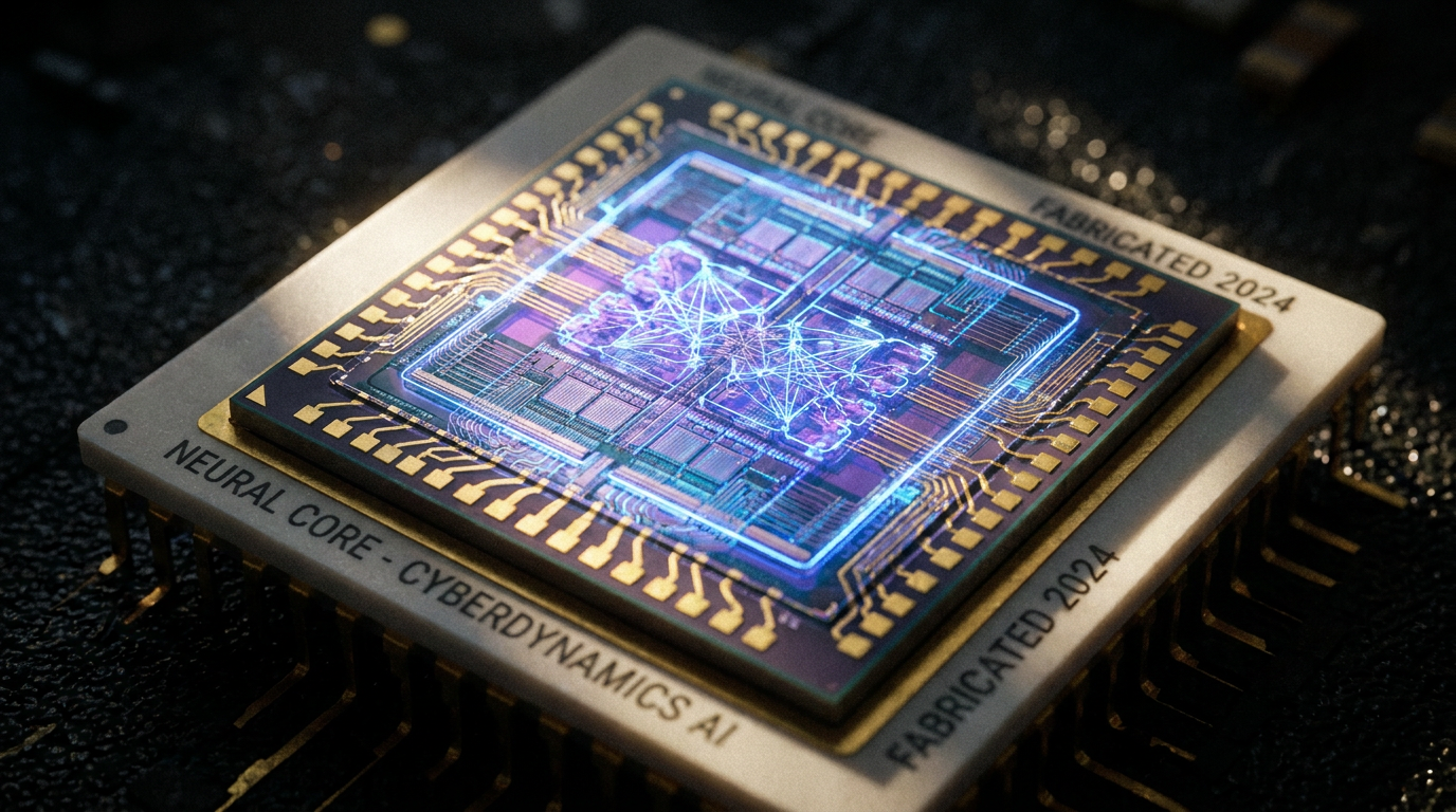
Toronto-based startup Taalas has unveiled a custom AI chip that physically bakes the Llama 3.1 8B model into silicon, achieving unprecedented inference speeds of 17,000 tokens per second. By eliminating the 'memory wall' that bottlenecks traditional GPUs, the HC1 chip promises to drastically reduce the cost and energy footprint of AI deployment.
By Factlen Editorial Team
- Specialized Hardware Advocates
- Argue that deep specialization is the only viable path to overcoming the energy and cost limits of general-purpose GPUs.
- General-Purpose Compute Defenders
- Point out that AI models evolve too rapidly for hardwired silicon, risking rapid obsolescence.
- Edge Computing Proponents
- Excited about the potential to run frontier models locally without cloud dependency.
What's not represented
- · Major GPU Manufacturers (Nvidia/AMD)
- · Cloud Service Providers
Why this matters
If AI models can be printed directly onto chips for a fraction of the cost and power of general-purpose GPUs, it could democratize access to high-performance AI. This breakthrough enables instant real-time agents and massive cost reductions for data centers, potentially bifurcating the hardware market.
Key points
- Startup Taalas has developed the HC1, a custom chip that physically hardwires the Llama 3.1 8B model into silicon.
- The chip achieves inference speeds of 17,000 tokens per second, nearly 10 times faster than the current state-of-the-art.
- By eliminating external memory, the HC1 draws 10 times less power and costs 20 times less to manufacture than traditional GPUs.
- The chip trades flexibility for speed; it cannot run any other model, though it supports fine-tuning via programmable SRAM.
- Taalas plans to release a second-generation chip supporting standard 4-bit floating-point formats and larger models by winter 2026.
The fundamental bottleneck in modern artificial intelligence is not the speed of computation, but the commute. In traditional GPU architectures, the vast majority of time and energy is spent shuttling data back and forth between the memory where an AI model's weights are stored and the processing cores where the math happens. This phenomenon, known as the 'memory wall,' limits how fast large language models can generate text and drives up the massive power requirements of AI data centers.[1][6]
Toronto-based startup Taalas has introduced a radical solution to this bottleneck: eliminating the memory entirely. Emerging from stealth in early 2026, the company unveiled the HC1, an application-specific integrated circuit (ASIC) that physically hardwires the open-source Llama 3.1 8B model directly into the silicon. Instead of loading the model from external memory banks into a generalized processor, the model and the chip are one and the same. By baking the neural network directly into the physical structure of the processor, Taalas is fundamentally rewriting the architecture of artificial intelligence hardware.[3][7]
The performance results of this extreme specialization are staggering. In live demonstrations, the HC1 chip achieves inference speeds of roughly 17,000 tokens per second per user. To put that in perspective, an Nvidia H200 GPU manages a few hundred tokens per second on the same model, while specialized SRAM-based chips from Groq and Cerebras hit roughly 600 and 2,000 tokens per second, respectively. By removing the memory commute, Taalas is delivering nearly an order of magnitude more throughput than the fastest competing hardware currently available on the market.[2][3][7]

The company behind the breakthrough was founded by a team of engineers with deep roots in silicon design, led by former Tenstorrent co-founder Ljubisa Bajic. Despite raising over $200 million from investors including Quiet Capital and Fidelity, Taalas spent only $30 million and utilized a highly focused team of just 24 people to bring the HC1 from concept to working silicon in under three years. This capital efficiency stands in stark contrast to the billions typically required to develop new semiconductor architectures.[2][4][7]
The mechanism powering the HC1 relies on a technology called mask ROM. During the manufacturing process at TSMC's 6-nanometer fabrication plants, the model's weights are physically etched into the metal layers of the chip. The HC1 packs 53 billion transistors onto an 815-square-millimeter die, effectively turning the 32 layers of the Llama 3.1 model into a sequential physical pathway. Because the data is permanently written into the hardware, it cannot be altered or erased once the chip leaves the foundry.[3][5]
When a user submits a prompt, the data does not cycle through a central processor. Instead, the electrical signals flow continuously down physical wires from the first layer of transistors to the next, streaming through the silicon until the final output token is generated. To make this continuous flow possible, Taalas developed a novel hardware scheme that allows a single transistor to store data and perform the associated matrix multiplication simultaneously. This 'magic multiplier' approach dramatically reduces the physical footprint required for computation and keeps the data moving forward without interruption.[5][6]
This continuous flow architecture eliminates the need for High Bandwidth Memory (HBM), advanced liquid cooling systems, and complex packaging techniques. As a result, a single HC1 card draws only about 200 watts of power. A standard air-cooled server rack holding ten of these cards consumes just 2.5 kilowatts, a fraction of the power required by traditional GPU clusters. Beyond the energy savings, the simplified architecture means the chips cost an estimated 20 times less to manufacture than flagship AI processors.[3][6][7]

This continuous flow architecture eliminates the need for High Bandwidth Memory (HBM), advanced liquid cooling systems, and complex packaging techniques.
However, this extreme efficiency comes with a severe trade-off: zero flexibility. The HC1 can only run Llama 3.1 8B. It cannot run a different model architecture, nor can the base weights of the hardwired model be updated with new training data. In an industry where state-of-the-art models are superseded every few months, hardwiring a specific model into silicon risks rapid obsolescence. Critics point out that this rigid design forces customers to completely replace their physical hardware whenever a superior artificial intelligence model is released, rather than simply downloading a software update.[1][2]
Taalas argues that the underlying economics of their manufacturing approach neutralize this risk of obsolescence. Because their design only requires customizing two of the chip's metal layers to encode a new model, fabricating an updated chip takes roughly two months from start to finish. The company estimates that printing a new batch of chips costs approximately 1 percent of what it cost to train the model in the first place. At that price point, Taalas believes that physical hardware replacement becomes a financially viable alternative to traditional software updates.[3][5]
Furthermore, the HC1 is not entirely rigid in its deployment. The chip includes a small amount of programmable Static Random-Access Memory (SRAM) used for the KV cache and to store Low-Rank Adaptations, commonly known as LoRAs. This hybrid approach allows developers to fine-tune the model's behavior, adjust context windows, and customize responses for specific enterprise applications without altering the physically etched base weights. By supporting these adapters, Taalas provides just enough flexibility to make the chip useful across a variety of different software environments while maintaining its blistering speed.[1][2]
To fit the entire 8-billion-parameter model onto a single 6-nanometer chip, Taalas had to make significant compromises on mathematical precision. The 'Silicon Llama' is aggressively quantized, using a custom combination of 3-bit and 6-bit parameters rather than the standard high-precision formats typically used in data centers. The company openly acknowledges that this low-precision format introduces some quality degradation compared to running the uncompressed model on a traditional GPU. While the text generation remains highly coherent, the aggressive quantization makes the first-generation chip less suitable for tasks requiring absolute mathematical exactness.[2][5]

Taalas views the HC1 primarily as a technology demonstrator rather than a final commercial product meant for mass deployment. The company is already deep into developing its second-generation silicon platform, the HC2, which will adopt standard 4-bit floating-point formats to resolve the accuracy limitations while maintaining the architecture's high speed. By moving the SRAM onto separate chips, the next generation will enable far greater memory density, paving the way for much larger and more capable artificial intelligence models to be hardwired into silicon without sacrificing response quality.[1][5]
The roadmap for the HC2 architecture includes supporting much larger models by distributing the compute load across multiple synchronized chips. Taalas plans to deploy a mid-sized reasoning model by the summer of 2026 and aims to have a frontier-class large language model running on hardwired silicon by the winter. Internal simulations suggest that running a massive, 671-billion-parameter model like DeepSeek R1 across 30 synchronized chips could still achieve an astonishing 12,000 tokens per second, proving that the hardwired approach can scale to the absolute cutting edge of artificial intelligence.[1][4]
The introduction of hardwired models represents a new frontier in the ongoing artificial intelligence hardware race. While companies like Etched are building ASICs optimized specifically for the Transformer architecture, and Groq is maximizing SRAM speed for deterministic execution, Taalas is the first to completely merge the software model with the physical hardware. This approach trades the safety of general-purpose computing for the ultimate extreme of specialized performance, challenging the fundamental assumptions of how data centers should be built and operated in the age of generative artificial intelligence.[1][6][7]

If Taalas can successfully scale this approach to frontier models, it could fundamentally bifurcate the global compute market. General-purpose GPUs would remain the undisputed standard for training new models and conducting open-ended research, while hardwired ASICs could dominate the deployment of mature models at scale. By slashing the cost and energy required for inference, this technology could enable real-time, low-latency AI agents to run locally on edge devices, democratizing access to high-performance artificial intelligence across the globe and breaking the monopoly of massive, liquid-cooled data centers.[1][6]
How we got here
2023
Taalas is founded by a team of engineers led by former Tenstorrent co-founder Ljubisa Bajic.
Late 2025
Taalas begins manufacturing the HC1 chip, hardwiring the open-source Llama 3.1 8B model into silicon.
Feb 2026
Taalas emerges from stealth, releasing the HC1 chip and a public demonstration achieving 17,000 tokens per second.
Summer 2026
Expected release of a mid-sized reasoning model running on the first-generation HC1 silicon platform.
Winter 2026
Planned deployment of the second-generation HC2 silicon, designed to support frontier-class large language models.
Viewpoints in depth
Specialized Hardware Advocates
Argue that deep specialization is the only viable path to overcoming the energy and cost limits of general-purpose GPUs.
This camp emphasizes that the history of computing always trends toward specialization for critical workloads. Just as Bitcoin mining transitioned from CPUs to GPUs and finally to ASICs, they believe AI inference must follow the same path. By eliminating the memory wall, hardwired chips offer a leap in efficiency that general-purpose hardware physically cannot match, making it the only sustainable way to deploy AI at a global scale.
General-Purpose Compute Defenders
Point out that AI models evolve too rapidly for hardwired silicon, risking rapid obsolescence.
Critics of the hardwired approach argue that the AI landscape is too volatile for fixed-function chips. With state-of-the-art models being superseded every few months, a chip that takes two months to manufacture could be outdated by the time it reaches the data center. They maintain that the flexibility of GPUs—which can run any new architecture or model size instantly—justifies their higher power consumption and cost.
Edge Computing Proponents
Excited about the potential to run frontier models locally without cloud dependency.
For developers focused on edge devices, the massive reduction in power and cost is a game-changer. If a powerful language model can run on a 200-watt card without requiring liquid cooling or complex memory packaging, it opens the door to embedding high-performance AI directly into vehicles, industrial robots, and local enterprise servers, entirely removing the latency and privacy concerns of cloud-based inference.
What we don't know
- How the hardwired approach will scale to massive frontier models like DeepSeek R1, which would require synchronizing dozens of chips.
- Whether the two-month manufacturing turnaround for new chips will be fast enough to keep pace with the rapid release cycle of new AI models.
- How much the aggressive quantization required for the first-generation chip impacts the model's performance in real-world, complex reasoning tasks.
Key terms
- Memory Wall
- The performance bottleneck caused by the time and energy required to move data between a computer's memory and its processing cores.
- Application-Specific Integrated Circuit (ASIC)
- A microchip designed for a specific, narrow application rather than general-purpose computing.
- Mask ROM
- Read-only memory where the data is physically written into the integrated circuit during manufacturing and cannot be changed.
- Quantization
- The process of reducing the precision of an AI model's weights to save memory and compute resources, sometimes at the cost of slight accuracy degradation.
- Inference
- The phase where a trained AI model is put to work generating responses or predictions based on new input data.
Frequently asked
Can the Taalas chip run different AI models?
No, the HC1 chip is physically hardwired to run only the Llama 3.1 8B model. The model's weights are etched into the silicon itself.
How does it achieve 17,000 tokens per second?
By eliminating the 'memory wall.' Data flows continuously through the chip's physical transistors without needing to be fetched back and forth from external memory banks.
What happens when a better AI model is released?
A completely new chip must be manufactured. Taalas claims this process takes about two months and costs only a fraction of the model's original training cost.
Can the hardwired model be fine-tuned?
Yes, the chip includes a small amount of programmable SRAM that supports Low-Rank Adaptation (LoRA), allowing developers to adjust the model's behavior without changing the base weights.
Sources
Source coverage
7 outlets
3 viewpoints surfaced


[1]ForbesSpecialized Hardware Advocates
Taalas Hardcore AI: Hardened AI Models
Read on Forbes →[2]EE TimesGeneral-Purpose Compute Defenders
Taalas Hardwires Llama 3.1 Into Silicon for 17,000 Tokens/s
Read on EE Times →[3]SiliconAngleGeneral-Purpose Compute Defenders
Taalas raises $169M in funding to develop model-specific AI chips
Read on SiliconAngle →[4]Silicon RepublicEdge Computing Proponents
Canadian start-up chipmaker Taalas raises $169m
Read on Silicon Republic →[5]TaalasEdge Computing Proponents
The path to ubiquitous AI
Read on Taalas →[6]WCCFTechSpecialized Hardware Advocates
Taalas Manages to Achieve 10x Higher TPS With Meta's Llama 8B LLM, That Too With 20x Lower Production Costs
Read on WCCFTech →[7]MediumEdge Computing Proponents
When Your Model IS the Chip
Read on Medium →

Every angle. Every day.
Get ai stories with full source coverage and perspective breakdowns delivered to your inbox.