Samsung and SK Hynix Announce $518 Billion Chipmaking Hub to Meet Global AI Demand
South Korea's two memory giants will invest 800 trillion won to build a massive semiconductor cluster in the country's southwest, aiming to double AI chip production capacity within five years.
By Factlen Editorial Team
- Global AI Supply Chain Analysts
- Views the investment through the lens of market demand, focusing on how it will alleviate the long-term hardware bottleneck for AI hyperscalers.
- National Industrial Planners
- Focuses on securing South Korea's global technological dominance while promoting balanced regional economic development.
- Infrastructure Skeptics
- Raises concerns about the logistical feasibility of powering and supplying water to massive fabs in a region reliant on intermittent renewable energy.
What's not represented
- · Local Honam region residents
- · Environmental groups monitoring water usage
- · Chinese semiconductor competitors
Why this matters
The global AI boom is entirely dependent on a constrained supply of high-bandwidth memory chips. This unprecedented half-trillion-dollar expansion signals that the hardware shortage could ease in the coming years, stabilizing prices for everything from enterprise AI accelerators to consumer electronics.
Key points
- Samsung and SK Hynix will invest $518 billion to build four new semiconductor fabrication plants in South Korea's southwest.
- The investment aims to double the nation's AI memory chip production capacity within five years.
- The new hub shifts manufacturing away from the crowded Seoul region to tap into the southwest's renewable energy and land.
- The facilities will focus on High-Bandwidth Memory (HBM) and advanced packaging, critical components for AI data centers.
- Critics warn that the region's intermittent renewable power and strained water dams pose significant execution risks.
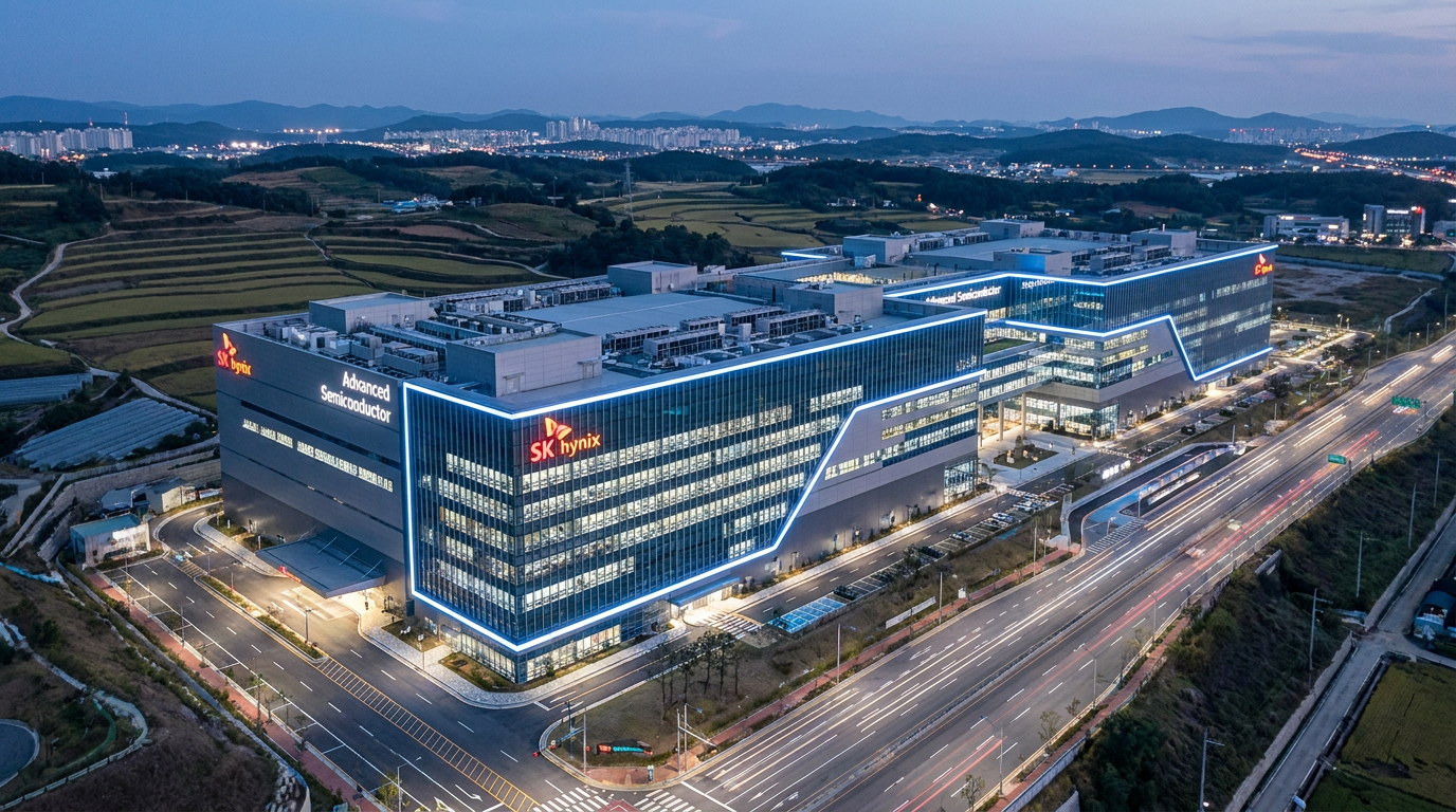
The global race to build artificial intelligence infrastructure just triggered the largest industrial investment in South Korean history. On Monday, tech giants Samsung Electronics and SK Hynix announced an unprecedented, combined 800 trillion won ($518 billion) commitment to construct a sprawling new semiconductor manufacturing hub in the country's southwest region. The move represents a massive escalation in the capital required to compete in the modern tech economy, signaling that the era of relatively cheap, ubiquitous computing power is giving way to highly specialized, capital-intensive mega-projects.[1][2]
The sheer scale of the initiative, unveiled alongside President Lee Jae-myung, underscores the intense pressure currently squeezing the global hardware supply chain. The two companies, which already produce roughly two-thirds of the world's memory chips, plan to build four massive new fabrication plants dedicated exclusively to advanced memory and packaging. This is not merely an expansion of existing product lines; it is a fundamental rewiring of their manufacturing footprint to meet the insatiable demands of artificial intelligence developers worldwide.[1][5]
During the televised announcement, President Lee framed the half-trillion-dollar investment as a national imperative rather than a simple corporate expansion. 'Speed is the only path to survival,' he declared, describing semiconductors, physical AI, and AI data centers as the 'triple axis' for South Korea's economic future. The government is heavily backing the initiative, viewing it as essential to maintaining the country's technological sovereignty in an era where silicon has become as strategically vital as oil. By aligning state resources with private capital, Seoul is attempting to outmaneuver rival nations that are also subsidizing their domestic chip industries.[7]

To understand the necessity of this staggering financial bet, one must look closely at the architecture of modern artificial intelligence. Generative AI models like ChatGPT and Claude rely on massive clusters of Graphics Processing Units (GPUs) to train their neural networks. However, those powerful processors are effectively useless without High-Bandwidth Memory (HBM) chips to feed them massive datasets at lightning speeds. As AI models grow exponentially larger, the bottleneck has shifted from the processing cores to the memory bandwidth, creating a desperate scramble for HBM supply.[5][8]
Manufacturing High-Bandwidth Memory is not a simple matter of printing more silicon. It involves stacking multiple memory chips vertically and connecting them with microscopic wires through a highly complex process known as advanced packaging. SK Hynix made an early, aggressive bet on this specific HBM architecture years ago, a strategic gamble that recently propelled it past Samsung to become South Korea's most valuable listed company. Now, both conglomerates are racing to scale up their advanced packaging capabilities before the next generation of AI models requires even more bandwidth.[5][8]
This AI-driven memory supercycle has fundamentally changed the semiconductor business model. Historically, memory chipmakers mass-produced generic components and sold them on the open market, leading to volatile boom-and-bust cycles. Today, the industry is shifting to a 'customer order-based production' system, where chips are custom-optimized and packaged for specific hyperscalers like Microsoft, Amazon, and Google. This bespoke manufacturing requires significantly more physical space, specialized equipment, and tighter integration with the end-customer's hardware designs. The new Honam hub is explicitly designed to accommodate this shift, providing the vast cleanroom floors needed for customized advanced packaging lines.[6][8]

Currently, South Korea's semiconductor industry is heavily concentrated in the greater Seoul metropolitan area, specifically within the massive Yongin and Pyeongtaek clusters. However, those existing sites are rapidly approaching their absolute physical and infrastructural limits. Semiconductor fabrication is incredibly resource-intensive, and the Seoul-adjacent hubs are running out of available land, hitting the ceiling on power consumption, and exhausting local water supplies. Expanding further in the capital region is no longer a viable option for the scale of growth AI demands.[3][4]
However, those existing sites are rapidly approaching their absolute physical and infrastructural limits.
By shifting this new mega-cluster to the Honam region in the southwest—specifically targeting areas around Gwangju and the Jeolla provinces—the government is attempting to solve two massive problems simultaneously. First, it relieves the severe industrial bottleneck choking the capital region. Second, it fulfills a long-standing political pledge to bring balanced economic development to historically underserved areas. The southwest has traditionally lagged behind the capital in high-tech investment, making this project a cornerstone of the administration's regional equity platform.[1][7]
Beyond politics, the southwest offers distinct logistical advantages for the future of tech manufacturing. The Honam region features vast tracts of available land and, crucially, a significantly higher concentration of renewable energy infrastructure. As global tech giants face increasing regulatory and public pressure to decarbonize their supply chains, the ability to power energy-hungry fabs with clean electricity has become a major competitive advantage. Apple, Microsoft, and Google are increasingly demanding that their suppliers utilize green energy, making the southwest's solar and wind resources highly attractive.[1][3]

The timeline for the mega-cluster is incredibly aggressive, reflecting the urgency of the AI boom. Officials are targeting a completion window of 2034 to 2035, accelerating previous regional development plans by more than a decade. In the interim, Samsung and SK Hynix are pushing to double the nation's overall DRAM production capacity within the next five years. This phased approach is designed to provide immediate relief to the market while laying the groundwork for the massive new facilities in the southwest.[5][6]
If successful, the Honam cluster will cement South Korea's absolute dominance in cutting-edge memory processes for the next generation. Industry analysts note that this overwhelming capacity expansion is also a calculated defensive maneuver. By investing half a trillion dollars into advanced AI memory, South Korea aims to build an insurmountable technological lead over emerging Chinese competitors, who are currently aggressively expanding their footprint in the older, legacy chip market. The strategy is to abandon the low end and monopolize the high-margin future.[4][6]
However, executing a $518 billion infrastructure project is fraught with severe logistical hurdles. Semiconductor fabrication requires staggering amounts of ultra-pure water and uninterrupted, 24/7 electricity. The manufacturing tolerances are so precise that a single power blip lasting a fraction of a second can ruin millions of dollars worth of silicon wafers and damage highly sensitive lithography equipment. Ensuring that the new southwest hub has the flawless utility backbone required for this level of manufacturing is a monumental civil engineering challenge.[3][6]
Infrastructure skeptics have already raised alarms about the Honam region's readiness to host such demanding facilities. While the area boasts abundant renewable energy, solar and wind power are inherently intermittent. Currently, nearly half of the region's power generation comes from these variable sources, which cannot reliably sustain a mega-fab's continuous baseload requirements without massive, grid-scale battery storage or the construction of new nuclear power plants. Balancing the desire for green energy with the reality of fab power consumption remains an unsolved puzzle.[6]
Furthermore, water resources in the Jeolla provinces are already heavily strained, with local dams frequently operating near their maximum capacity just to serve existing agricultural and municipal needs. Supplying the millions of gallons of daily ultra-pure water required for four new semiconductor fabs will require significant new water management infrastructure, including potential desalination plants or massive new reservoirs. Critics warn that without these parallel investments, the fabs could become stranded assets. The environmental impact of diverting such massive water resources is also likely to draw intense scrutiny as the project moves from the planning phase to breaking ground.[3][6]

There is also the critical challenge of human capital. During the announcement, SK Hynix Chairman Chey Tae-won explicitly noted that the project requires not just vast sites and utilities, but an army of highly skilled engineers and technicians. Convincing top-tier talent to relocate from the vibrant Seoul metropolitan area to the more rural southwest has historically been a major struggle for Korean conglomerates. The companies will likely need to build entire supporting ecosystems, including international schools and luxury housing, to attract the necessary workforce.[1][5]
Despite these formidable execution risks, the global market reaction has been overwhelmingly focused on the long-term relief this capacity will bring to the AI sector. The announcement signals the beginning of what financial analysts are calling the 'Mega Investment Era,' a period where sovereign nations and tech giants pool their vast resources to build the physical foundation of the AI economy. It is a recognition that software innovation has outpaced hardware reality, and catching up requires unprecedented capital. The sheer size of the commitment provides a stabilizing signal to the broader tech industry.[6][8]
For the global supply chain, the message from Seoul is clear: the hardware shortage may persist in the near term, but the cavalry is coming. South Korea is betting its industrial future on the premise that the world's appetite for artificial intelligence has only just begun. By committing half a trillion dollars to the Honam mega-cluster, Samsung and SK Hynix are not just responding to current demand; they are actively building the infrastructure that will make the next decade of AI breakthroughs physically possible.[4][7]
How we got here
2022–2023
The launch of ChatGPT triggers a massive surge in demand for High-Bandwidth Memory (HBM) chips, catching the broader market off guard.
2024–2025
SK Hynix capitalizes on its early HBM investments, surpassing Samsung in market value and becoming Nvidia's primary memory supplier.
Early 2026
Existing South Korean semiconductor hubs in Yongin and Pyeongtaek approach their physical and infrastructural limits.
June 29, 2026
Samsung and SK Hynix officially announce the $518 billion Honam mega-cluster to double capacity.
2034–2035
Target completion window for the four new fabrication plants in the southwest region.
Viewpoints in depth
National Industrial Planners
South Korean officials view the mega-cluster as a dual-purpose victory for both global competitiveness and domestic equity.
For the government, the $518 billion investment is about securing the 'triple axis' of the future economy: semiconductors, physical AI, and data centers. By forcing this development into the Honam region, planners hope to break the Seoul metropolitan area's monopoly on high-tech jobs, utilizing untapped land and renewable energy to revitalize the southwest.
Global AI Supply Chain Analysts
Market observers see the expansion as a necessary, albeit delayed, relief valve for the AI hardware bottleneck.
Analysts emphasize that the shift to 'customer order-based production' for High-Bandwidth Memory requires unprecedented scale. While the new fabs won't solve the immediate 2026 chip shortage, the commitment of half a trillion dollars provides long-term certainty to hyperscalers like Microsoft and Google that the physical infrastructure of AI will continue to scale.
Infrastructure Skeptics
Critics warn that the southwest region lacks the reliable utilities required for 24/7 semiconductor fabrication.
Skeptics point out that advanced fabs cannot run on intermittent renewable energy alone. With Honam's power grid heavily reliant on solar and wind, and local water dams already operating at high capacity, critics argue that the government must undertake massive, parallel civil engineering projects to prevent the mega-cluster from becoming a stranded asset.
What we don't know
- How the government plans to supply the massive baseload power required without relying entirely on intermittent renewables.
- Whether the companies can successfully convince enough highly skilled engineers to relocate to the southwest region.
- The exact timeline for when the first commercial chips will roll off the new Honam assembly lines.
Key terms
- High-Bandwidth Memory (HBM)
- A specialized type of computer memory that stacks chips vertically to process massive amounts of data at high speeds, essential for AI processors.
- Advanced Packaging
- The highly complex manufacturing process of connecting multiple microscopic chips together into a single, tightly integrated component.
- Fabrication Plant (Fab)
- A highly controlled, multi-billion-dollar manufacturing facility where silicon wafers are turned into integrated circuits.
- Hyperscaler
- Massive technology companies, such as Amazon, Google, and Microsoft, that operate global networks of massive data centers.
Frequently asked
Why are Samsung and SK Hynix investing so much money?
The global boom in artificial intelligence requires massive amounts of specialized memory chips. The companies are investing $518 billion to double their production capacity and maintain their dominance in the global supply chain.
Why is the new hub being built in the southwest?
Existing chipmaking hubs near Seoul are running out of space, power, and water. The southwest Honam region offers available land, renewable energy resources, and aligns with the government's goal of balanced regional development.
Will this fix the current chip shortage?
Not immediately. Building semiconductor fabs takes years. The new facilities are targeted for completion between 2034 and 2035, meaning this investment is aimed at securing the long-term future of AI hardware rather than providing short-term relief.
Sources
Source coverage
8 outlets
3 viewpoints surfaced


[1]AP NewsNational Industrial Planners
South Korean tech giants to build a $518 billion chipmaking hub to serve soaring AI demand
Read on AP News →[2]India TodayGlobal AI Supply Chain Analysts
Samsung, SK Hynix to invest $518 billion in South Korea chip hub
Read on India Today →[3]The ElecInfrastructure Skeptics
Controversy Brews Over Samsung, SK hynix's Potential Honam Semiconductor Mega Cluster
Read on The Elec →[4]Seoul Economic DailyNational Industrial Planners
Samsung, SK hynix to Pour 3,530 Trillion Won Into Chip Mega-Cluster
Read on Seoul Economic Daily →[5]KED GlobalGlobal AI Supply Chain Analysts
Samsung, SK Hynix to build new chip cluster, boost packaging and NAND capacity
Read on KED Global →[6]Let's Data ScienceInfrastructure Skeptics
South Korea's 800 Trillion Won Semiconductor Cluster Faces Execution Risks
Read on Let's Data Science →[7]TBS NewsNational Industrial Planners
South Korea rolls out sweeping AI, chip mega-projects
Read on TBS News →[8]BloombergGlobal AI Supply Chain Analysts
Samsung, SK Hynix at Center of South Korea's AI Drive
Read on Bloomberg →


Every angle. Every day.
Get technology stories with full source coverage and perspective breakdowns delivered to your inbox.