
IBM Unveils World's First Sub-1nm Chip With 'Nanostack' Architecture, Promising 50% Performance Boost for AI
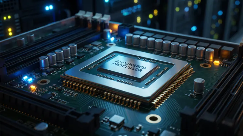
IBM has demonstrated the first functioning 0.7-nanometer chip, utilizing a 3D 'nanostack' architecture to pack 100 billion transistors into the size of a fingernail. The breakthrough could dramatically reduce the power demands of AI data centers, though commercial production remains years away.
By Sofia Matos

- Semiconductor Researchers
- Focus on overcoming the physical limits of Moore's Law and extending compute scaling.
- Enterprise AI Infrastructure
- Focus on the economic and energy implications of denser, more efficient compute.
- Hardware Pragmatists
- Emphasize the long timeline and manufacturing hurdles between research and mass production.
Perspectives this story doesn't cover
- Foundry Operators (TSMC, Samsung, Intel) tasked with manufacturing the design
- Environmental groups monitoring data center energy consumption
Summary
- IBM has unveiled the world's first sub-1 nanometer chip, utilizing a 0.7nm (7 angstrom) node.
- The new 'nanostack' architecture builds transistors vertically in 3D, rather than shrinking them on a flat plane.
- The design packs 100 billion transistors onto a fingernail-sized chip, doubling the density of IBM's 2021 2nm breakthrough.
- The chips are projected to deliver 50% more performance or use 70% less energy, directly targeting the power demands of AI.
For two decades, the semiconductor industry has been racing toward a physical wall: the point at which transistors become so small that the laws of physics stop cooperating. As features shrink to the width of a few atoms, electrons begin to leak, and the steady drumbeat of Moore's Law—the historical doubling of computing power every two years—has slowed to a crawl.[1]
Now, IBM claims to have found a way over that wall. The company has unveiled the world's first sub-1 nanometer chip technology, demonstrating a working prototype at the 0.7-nanometer (or 7 angstrom) node.
The breakthrough allows engineers to pack approximately 100 billion transistors onto a piece of silicon roughly the size of a human fingernail. This represents nearly twice the density of the 2-nanometer architecture IBM introduced in 2021.[1]
According to published technical results, the new design promises a substantial leap in capability. Chips built on this node are projected to deliver up to 50 percent more performance than current 2-nanometer chips, or alternatively, consume 70 percent less energy to perform the exact same workloads.
To achieve this, IBM had to abandon the traditional flat plane of chip design. The secret lies in a new architecture the company calls "nanostack." Rather than trying to cram more transistors side-by-side on a two-dimensional surface, nanostack builds upward, utilizing three-dimensional sequential integration.[1]
Historically, the industry has relied on FinFET and, more recently, Gate-All-Around (GAA) "nanosheet" designs to control electron flow in shrinking spaces. But even nanosheets have a limit; as they get thinner, they struggle to contain electrical leakage.
Nanostack shifts the paradigm to what the industry calls Complementary Field-Effect Transistor (CFET) technology. In a traditional layout, n-type and p-type transistors sit next to each other. IBM's nanostack vertically stacks and staggers them, resembling a high-density microscopic cityscape.
This vertical integration does more than just save space. Because the transistor layers are built separately and bonded together using an ultra-thin, non-conductive dielectric layer, engineers can mix and match different semiconductor materials within the same stack.
This means the performance and power efficiency of each individual transistor layer can be optimized independently, a level of granular control previously impossible in mass manufacturing.
The implications for artificial intelligence are profound. Modern AI models are notoriously power-hungry, driving massive investments in energy infrastructure and forcing tech giants to seek independent power sources for their data centers.[2]
A chip architecture that can cut energy consumption by 70 percent fundamentally alters the economics of AI. For enterprise infrastructure, denser and more efficient silicon translates directly to a plummeting cost-per-inference, making it cheaper to run complex models locally rather than renting cloud compute.[2]
Furthermore, the nanostack design directly addresses the memory bottlenecks that plague AI accelerators. At the VLSI 2026 symposium, researchers demonstrated that the architecture provides a 40 percent scaling improvement in SRAM—the fast, on-chip memory essential for feeding data-hungry AI workloads.[1]
IBM estimates that future AI accelerators utilizing 7-angstrom technology could deliver roughly 9,000 Trillions of Operations Per Second (TOPS), a six-fold increase over the 1,500 TOPS produced by today's leading hardware.
However, industry analysts caution that this is currently a research achievement, not a shipping product. The prototype proves the physics work—IBM has successfully demonstrated functional CMOS inverter operation—but mass manufacturing is a different beast entirely.[1]
Bringing nanostack chips to market will require overcoming immense engineering hurdles related to thermal management, advanced packaging, and large-scale integration. Stacking transistors vertically concentrates heat, which must be efficiently dissipated to prevent the chip from melting under heavy loads.
Commercial production is estimated to be at least five years away. It will rely heavily on next-generation supply chains, including the deployment of ASML's High-NA EUV lithography machines, which are required to print circuits at the atomic scale.[1][2]
IBM does not manufacture chips at scale itself; it licenses its designs. When foundries like TSMC, Intel, and Samsung see a viable sub-1nm architecture demonstrated, it accelerates the entire industry's roadmap, providing a clear target for the 2030s.[2]
For now, the successful demonstration of the nanostack architecture answers one of the most pressing questions in modern technology. It proves that the runway for compute scaling is longer than skeptics feared, ensuring that the hardware required to power the next decade of AI advancement can actually be built.[1]
Definitions
- Nanostack
- IBM's proprietary 3D chip architecture that vertically stacks and staggers transistors to increase density.
- Angstrom (Å)
- A unit of length equal to 0.1 nanometers, increasingly used to measure atomic-scale chip features.
- CFET
- Complementary Field-Effect Transistor, a design that stacks n-type and p-type transistors vertically rather than side-by-side.
- SRAM
- Static Random-Access Memory, fast on-chip memory crucial for feeding data to AI processors.
- Dielectric Bonding
- A technique using an ultra-thin, non-conductive insulating layer to bond separate transistor layers together.
Significance
As AI models grow exponentially larger, the energy required to train and run them is straining global power grids. By fundamentally changing how transistors are built, this architecture offers a viable path to keep scaling compute power without a proportional explosion in electricity use.
Sources
Source coverage
2 outlets
3 viewpoints surfaced


- [1]ForbesEnterprise AI Infrastructure
IBM Unveils World's First Sub-1nm Chip With 100 Billion 3D-Stacked Transistors
Read on Forbes → - [2]ibl.aiEnterprise AI Infrastructure
The Nanometer Barrier Is Broken: What IBM's NanoStack Means for Enterprise AI
Read on ibl.ai →
Comments

More in Artificial Intelligence
See all →AI Infrastructure
How FlashAttention Bypasses the GPU Memory Bottleneck to Enable Long-Context AI
5 sources
Open Source Standards
How the Open Source Initiative's 1.0 Definition Excludes the Most Downloaded Open-Weight AI Models
7 sources

Generative Adversarial Networks
How a Generator and a Discriminator Compete to Create Realistic AI Output
8 sources

Machine Learning
How Generative AI Maps the Joint Probability Distribution of Data
5 sources

Every angle. Every day.
Get Artificial Intelligence stories with full source coverage and perspective breakdowns delivered to your inbox.