South Korea Unveils $1.2 Trillion Investment Drive for AI and Semiconductor Industries
South Korea has announced a historic public-private initiative to build new semiconductor fabrication plants and AI data centers, aiming to secure its dominance in the global tech supply chain while shifting industrial development away from Seoul.
By Factlen Editorial Team
- Semiconductor Industry
- Sees the massive capital injection as necessary to maintain their near-monopoly on High-Bandwidth Memory (HBM) amid surging global demand.
- South Korean Government
- Views the initiative as a dual mandate to secure global AI dominance while forcing balanced regional development away from Seoul.
- Infrastructure Analysts
- Warns that building cutting-edge fabs in the southwest faces severe execution risks due to water shortages and a reliance on intermittent renewable energy.
What's not represented
- · Local residents of the Honam region
- · Environmental groups monitoring water and power usage
Why this matters
South Korea produces the vast majority of the high-bandwidth memory chips required to run global AI systems. This massive infrastructure expansion guarantees the long-term supply of these critical components, directly impacting the future cost and availability of AI technology worldwide.
Key points
- South Korea announced a $1.2 trillion public-private investment in AI and semiconductors.
- Samsung and SK Hynix will build four new fabrication plants in the southwestern Honam region.
- The plan aims to shift industrial development away from the overcrowded Seoul metropolitan area.
- The government will also invest heavily to expand AI data center capacity to 18.4 gigawatts by 2035.
- Infrastructure constraints, including water supply and intermittent renewable energy, pose significant execution risks.
South Korea has officially unveiled a staggering $1.2 trillion public-private investment initiative designed to cement its dominance in the global artificial intelligence and semiconductor supply chains. Announced on June 29, 2026, by President Lee Jae Myung, the "megaprojects" plan represents the largest industrial investment drive in the nation's history. The initiative is structured around a "triple axis" of advanced semiconductors, physical artificial intelligence, and massive AI data centers.[1][2]
The sheer scale of the capital commitment—equivalent to more than two-thirds of South Korea's gross domestic product—underscores the intense global arms race for AI hardware. As tech giants worldwide pour hundreds of billions into AI infrastructure, South Korea is leveraging its domestic corporate titans to ensure it remains the indispensable supplier of the memory chips that make modern AI possible.[3]
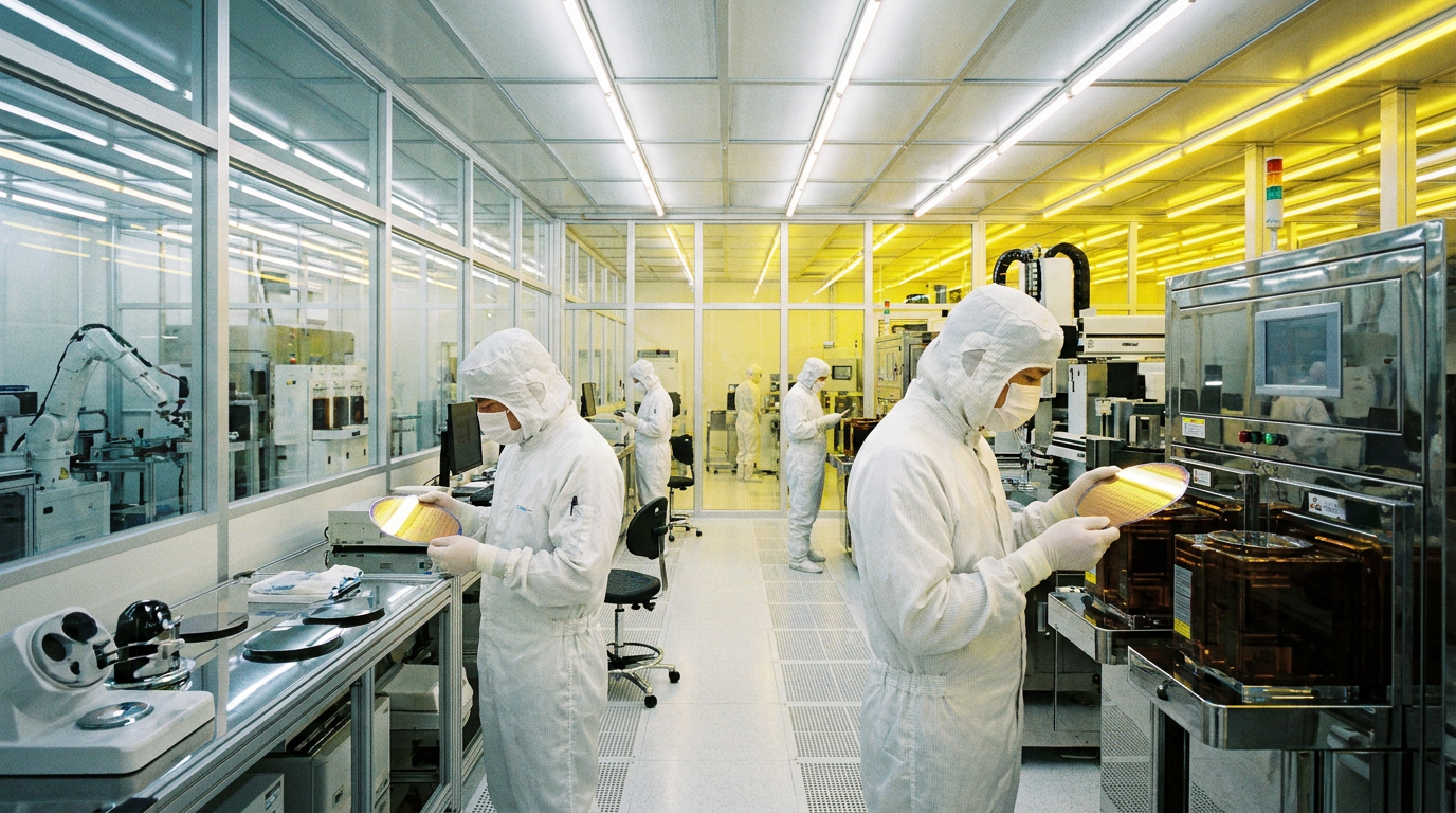
At the heart of the strategy is an 800 trillion won ($518 billion) commitment to build a sprawling new semiconductor manufacturing cluster. Samsung Electronics and SK Hynix, the world's two largest memory chipmakers, will lead the expansion by constructing four new fabrication plants. Unlike previous expansions, which clustered tightly around the capital, these new facilities will be built in the southwestern Honam region.[1][4]

The geographical shift is a central pillar of the government's strategy. For decades, South Korea's economic engine has been overwhelmingly concentrated in the Seoul metropolitan area, leading to severe overcrowding and regional inequality. Existing semiconductor hubs in Yongin and Pyeongtaek, located in Gyeonggi Province just outside Seoul, have effectively reached their physical and infrastructural limits.[2][5]
By directing the new 800 trillion won cluster to Gwangju and South Jeolla Province—which are slated to merge into a single special city—the administration aims to hit two targets at once: securing the land needed for massive new fabs while fulfilling a political pledge to drive balanced national development. President Lee emphasized that utilizing regional sites is now a "survival strategy" for the country.[2]
Complementing the primary fabrication hub in the southwest, the government has allocated an additional 81 trillion won to establish an advanced semiconductor packaging hub in the central Chungcheong region. Advanced packaging has become a critical battleground in the chip industry, as stacking and connecting different chiplets is now the primary method for increasing processing power and efficiency.[2]
The second major pillar of the $1.2 trillion initiative focuses on the infrastructure required to actually run artificial intelligence models. South Korea plans to invest roughly 1 quadrillion won ($650 billion) over the next decade to build a nationwide network of AI data centers.[3][5]
The second major pillar of the $1.2 trillion initiative focuses on the infrastructure required to actually run artificial intelligence models.
The data center rollout is aggressively phased. By 2029, the government and its corporate partners—including SK Group, GS Group, and Naver—aim to deploy 550 trillion won to achieve 8.4 gigawatts of AI data center capacity. By 2035, that capacity is projected to expand to a staggering 18.4 gigawatts, requiring an entirely new paradigm for national power generation and distribution.[2][3]

This massive domestic data center expansion serves a dual purpose. It ensures South Korea has the sovereign computing power necessary to develop its own AI models and physical AI robotics, while simultaneously creating a massive, captive domestic market for the high-end memory chips produced by Samsung and SK Hynix.[4]
The global context for this investment is the explosive demand for High-Bandwidth Memory (HBM). HBM chips are stacked memory modules that sit right next to the GPU in an AI server, feeding it data at lightning speeds. SK Hynix and Samsung currently dominate the global HBM market, and maintaining that near-monopoly is the primary economic driver behind the new fabrication plants.[1][4]
However, executing a $1.2 trillion industrial pivot away from the capital region carries severe logistical and infrastructural risks. Semiconductor fabrication plants are among the most resource-intensive facilities on earth, requiring absolute stability in power and massive volumes of ultra-pure water.[6]
Industry analysts have quickly pointed out the vulnerabilities in the Honam region's infrastructure. Water dams serving the Jeolla provinces are currently operating at 100% capacity, leaving little margin for the millions of gallons of daily industrial water the new fabs will require. While the government insists that supplying one million tons of industrial water per day is feasible, the engineering pathways remain complex.[3][6]

Power generation presents an even steeper hurdle. Semiconductor fabs must operate 24 hours a day, 7 days a week, without a single microsecond of power interruption. Currently, 47% of the Honam region's power generation comes from intermittent renewable sources like solar and wind. Bridging the gap between intermittent green energy and the baseload reliability required for chipmaking will necessitate massive grid upgrades.[6]
Beyond physical infrastructure, the human element remains a critical bottleneck. South Korea's highly skilled engineering workforce has historically been reluctant to relocate outside the Seoul metropolitan area, where the best schools, amenities, and professional networks are concentrated. Staffing four new cutting-edge fabs in the southwest will require significant financial incentives and regional development to attract top talent.[3]
Despite these hurdles, the South Korean government views the investment as an existential necessity. With the United States, Japan, and the European Union all heavily subsidizing their own domestic semiconductor industries, Seoul can no longer rely on its historical momentum. By streamlining permit approvals and accelerating construction timelines by up to a decade, South Korea is betting that speed and sheer scale will secure its place at the center of the AI revolution.[1][3]
How we got here
Early 2024
Global tech giants announce over $650 billion in AI infrastructure investments, sparking a race for hardware.
May 2026
South Korean officials debate how to distribute the massive tax revenues generated by the AI semiconductor boom.
June 29, 2026
President Lee Jae Myung officially unveils the $1.2 trillion 'megaprojects' initiative for chips and AI.
July 1, 2026
Gwangju and South Jeolla Province merge into a single special city to facilitate the new semiconductor cluster.
2034-2035
Target completion date for the new Honam region fabrication plants, accelerated by over a decade.
Viewpoints in depth
South Korean Government
Views the initiative as a dual mandate to secure global AI dominance while forcing balanced regional development away from Seoul.
For the administration, the $1.2 trillion investment is as much about domestic political economy as it is about global technology. By forcing the new semiconductor cluster into the historically neglected southwestern Honam region, the government aims to reverse decades of brain drain and overcrowding in the Seoul metropolitan area. Officials argue that streamlining permit approvals and accelerating construction timelines will allow South Korea to maintain its technological edge while simultaneously creating a more equitable national economy.
Semiconductor Industry
Sees the massive capital injection as necessary to maintain their near-monopoly on High-Bandwidth Memory (HBM) amid surging global demand.
Corporate giants like Samsung Electronics and SK Hynix are currently riding a wave of record profits driven by the AI boom, but they face intense pressure to scale up production. Their dominance in High-Bandwidth Memory (HBM) chips—the critical bottleneck for AI servers—requires constant, massive capital expenditure to stay ahead of rivals. For the industry, the government's willingness to subsidize infrastructure and fast-track approvals is the only way to build the capacity needed to satisfy the insatiable hardware demands of global tech companies.
Infrastructure Analysts
Warns that building cutting-edge fabs in the southwest faces severe execution risks due to water shortages and a reliance on intermittent renewable energy.
While the financial commitments are historic, infrastructure experts caution that the physical realities of the Honam region may delay or derail the project. Semiconductor fabrication plants require absolute stability in power and massive volumes of ultra-pure water. With local dams already operating at full capacity and nearly half of the region's power coming from intermittent renewable sources, analysts warn that the grid upgrades required to support 24/7 fab operations will be monumentally expensive and technically complex.
What we don't know
- Whether the Honam region can successfully upgrade its power grid to provide the uninterrupted baseload electricity required by 24/7 semiconductor fabs.
- How Samsung and SK Hynix plan to incentivize highly skilled engineers to relocate from the Seoul metropolitan area to the new southwestern cluster.
- The exact timeline for when the first silicon wafers will roll off the production lines at the new Honam facilities.
Key terms
- High-Bandwidth Memory (HBM)
- A specialized type of computer memory that stacks chips vertically, essential for the massive data processing required by AI graphics processing units (GPUs).
- Advanced Packaging
- The process of combining multiple semiconductor components into a single electronic package, crucial for boosting chip performance without shrinking transistors.
- Physical AI
- Artificial intelligence integrated into physical systems, such as advanced robotics and autonomous manufacturing equipment.
Frequently asked
Why is South Korea building fabs outside of Seoul?
Existing semiconductor hubs near Seoul have reached their spatial and infrastructural limits, and the government wants to use this massive investment to spur economic development in the historically neglected southwestern region.
Who is paying for the $1.2 trillion investment?
The initiative is a public-private partnership. The government is streamlining regulations and funding infrastructure, while corporate giants like Samsung Electronics and SK Hynix are providing the bulk of the direct capital for the facilities.
What are the main risks to the plan?
Analysts point to severe infrastructure constraints in the southwest, particularly the need for massive amounts of industrial water and consistent 24/7 electricity, which is difficult to guarantee in a region heavily reliant on intermittent renewable energy.
Sources
Source coverage
6 outlets
3 viewpoints surfaced


[1]ReutersSemiconductor Industry
South Korea unveils $576 bln chip investment to secure global dominance and rebalance growth
Read on Reuters →[2]The Korea HeraldSouth Korean Government
South Korea unveils blueprint for 3 flagship 'megaprojects' centered on AI, chips
Read on The Korea Herald →[3]Channel News AsiaSouth Korean Government
South Korea to invest nearly US$1.2 trillion in chips, AI data centres
Read on Channel News Asia →[4]The Straits TimesSemiconductor Industry
South Korea taps Samsung, SK Hynix in $745 billion plan to cement global AI chip lead
Read on The Straits Times →[5]Yahoo FinanceSemiconductor Industry
South Korea announces $1 trillion semiconductor and AI 'megaprojects' plan
Read on Yahoo Finance →[6]Let's Data ScienceInfrastructure Analysts
South Korea's 800 Trillion Won Semiconductor Cluster Faces Infrastructure Hurdles
Read on Let's Data Science →

Every angle. Every day.
Get world stories with full source coverage and perspective breakdowns delivered to your inbox.