
Caltech Breakthrough Achieves Fiber-Optic Efficiency on Silicon Chip
Researchers have engineered a new photonic integrated circuit that guides visible light with the ultralow signal loss of optical fiber, paving the way for chip-scale quantum sensors and highly efficient AI data centers.

Share this story
In short
- Caltech researchers have engineered silicon-based photonic circuits that guide visible light with the ultralow signal loss of optical fiber.
- The team used germano-silicate glass and a thermal reflow process to smooth waveguide surfaces to near-atomic levels.
- The platform achieves 20 times lower loss than conventional silicon nitride at visible wavelengths.
Silicon photonics has a visible-light problem. For decades, the technology that uses light to shuttle data between server racks has been confined to the infrared spectrum, where silicon is naturally transparent. When engineers try to push shorter, visible wavelengths through these chips, the light scatters and absorbs catastrophically. The rough edges of microscopic pathways act like physical speed bumps, dissipating the optical signal as heat and severely limiting the performance of precision devices.[1][2]
That wall has now crumbled. Researchers at the California Institute of Technology have engineered a new type of photonic integrated circuit that guides visible light with the same ultralow signal loss as a spool of optical fiber. By printing germano-silicate glass directly onto standard silicon wafers, the team has achieved a 20-fold reduction in optical loss compared to previous state-of-the-art materials.[2][3]
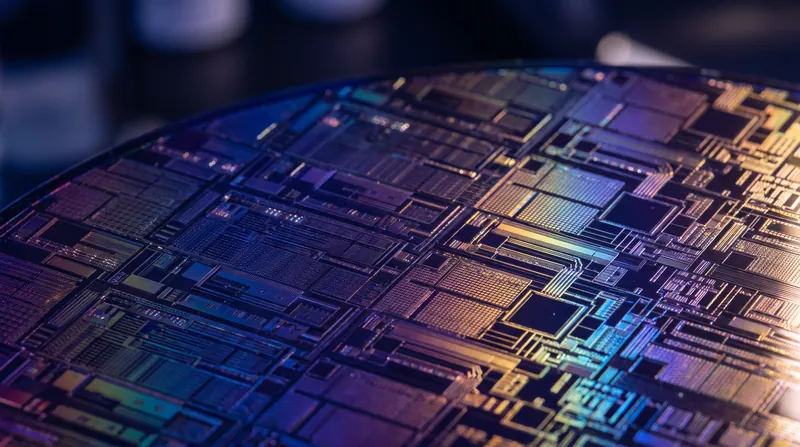
Optical fiber achieves its near-perfect transmission because it is made of exceptionally pure glass that is engineered to be extraordinarily smooth. To replicate this environment on a flat chip, the Caltech team utilized the exact same germano-silicate glass, but adapted it for a lithography-based manufacturing process that is fully compatible with standard 8-inch and 12-inch silicon wafers.[2]
The critical step in achieving this efficiency is a "thermal reflow" process. Because the germano-silicate material has a relatively low melting temperature, the researchers place the fabricated chips into a furnace. This gently melts the surface of the waveguides, smoothing out microscopic manufacturing imperfections down to the level of individual atoms. This atomic-level smoothness is what suppresses the severe scattering loss that previously plagued visible-light circuits.[1][2]
Space is another major constraint on a microchip. Instead of running the optical pathways in straight lines, the engineers arranged the waveguides in tight spirals. This geometry allows light to travel a much longer optical path—analogous to winding a long optical fiber around a spool—while remaining confined within a footprint smaller than a human fingernail.[2]
The data shows a dramatic leap in performance. At near-infrared wavelengths, the new platform matches the best existing devices made from silicon nitride. But at visible wavelengths, the germano-silicate waveguides outperform the previous silicon nitride record by a factor of 20. The platform achieves resonator Q factors—a measure of how long a device can store optical energy—surpassing 180 million across a spectrum ranging from violet to telecom wavelengths.[1][3]
This reduction in loss translates directly to device performance. For lasers built using these new ring resonators, the ability of light to circulate longer without scattering results in a more than 100-fold improvement in optical coherence. Highly coherent light is essential for precision measurements, as it maintains a stable frequency and phase over extended periods of time.[2][3]
The implications for quantum technology and metrology are profound. Precision instruments like optical clocks, which keep time based on the high-frequency ticking of atoms, and optical gyroscopes, which measure rotation for navigation, rely heavily on visible light. Previously, these systems required bulky, tabletop-sized optical setups. The Caltech breakthrough provides a pathway to shrink these laboratory-grade instruments onto a single, mass-producible chip.[1][3]
Beyond precision sensors, the technology addresses a looming crisis in artificial intelligence. The data centers powering large language models are increasingly bottlenecked not by raw computational power, but by the energy and heat required to transfer data between nodes using traditional copper wires. Replacing electrical interconnects with highly efficient, low-loss photonic circuits could drastically reduce the power consumption and latency of AI infrastructure.[3][4]
While the proof-of-concept is robust, the transition from a university laboratory to commercial foundries remains the next hurdle. The process relies on standard CMOS-compatible wafers, which is a significant advantage, but integrating the thermal reflow step into existing high-volume semiconductor manufacturing lines without damaging adjacent electronic components will require further engineering and thermal management.[1][4]
The researchers view this as a foundational shift rather than a final product. By marrying the performance benchmark of optical fibers with the mass-manufacturing scalability of silicon chips, integrated photonics is evolving from a specialized tool for telecommunications into a universal platform for next-generation computing and sensing.[2][4]
Key terms
- Photonic Integrated Circuit (PIC)
- A microchip that uses light (photons) instead of electricity (electrons) to process and transmit information.
- Waveguide
- A microscopic physical pathway etched into a chip that directs and confines the flow of light.
- Thermal Reflow
- A manufacturing process where a material is gently heated until it slightly melts, smoothing out microscopic surface imperfections.
- Resonator Q Factor
- A measurement of how efficiently an optical device can store light; a higher number means less energy is lost over time.
Viewpoints in depth
Photonic Engineers
Focus on the manufacturing scalability of printing germano-silicate on standard CMOS wafers.
For semiconductor engineers, the most significant aspect of the Caltech breakthrough is its compatibility with existing manufacturing infrastructure. By adapting germano-silicate glass for lithography on standard 8-inch and 12-inch wafers, the researchers have demonstrated that ultralow-loss photonics can be mass-produced. The thermal reflow process elegantly solves the surface roughness problem that has plagued the industry for years, offering a scalable path to commercialization without requiring entirely new fabrication facilities.
Quantum & Metrology Researchers
Emphasize the coherence improvements enabling chip-scale atomic clocks and quantum sensors.
Physicists and quantum researchers view the 100-fold improvement in laser coherence as a transformative capability. Precision instruments like atomic clocks and ion-trap quantum computers rely heavily on visible light and currently require large, vibration-isolated optical tables. The ability to achieve resonator Q factors of 180 million on a chip means these delicate, laboratory-grade quantum systems can finally be miniaturized into robust, portable devices, accelerating the deployment of quantum technologies in the field.
Computing & AI Analysts
Highlight the potential to solve bandwidth bottlenecks and energy loss in AI data centers.
From an infrastructure perspective, the breakthrough arrives at a critical moment for artificial intelligence. As AI models scale, the energy cost and thermal output of moving data electronically between processors are becoming unsustainable. Analysts note that replacing copper interconnects with highly efficient, low-loss photonic circuits could fundamentally alter data center architecture, enabling light-speed data transfer with near-zero energy loss and drastically reducing the power footprint of AI training clusters.
- Photonic Engineers
- Focus on the manufacturing scalability of printing germano-silicate on standard CMOS wafers.
- Quantum & Metrology Researchers
- Emphasize the coherence improvements enabling chip-scale atomic clocks and quantum sensors.
- Computing & AI Analysts
- Highlight the potential to solve bandwidth bottlenecks and energy loss in AI data centers.
Perspectives this story doesn't cover
- Commercial Semiconductor Foundries
Sources
Source coverage
4 outlets
3 viewpoints surfaced




- [1]NatureQuantum & Metrology Researchers
Towards fibre-like loss for photonic integration from violet to near-infrared
Read on Nature → - [2]Caltech NewsQuantum & Metrology Researchers
Extending Optical Fiber's Ultralow Loss Performance to Photonic Chips
Read on Caltech News → - [3]SciTechDailyPhotonic Engineers
Caltech Breakthrough Brings Fiber-Optic Performance to Silicon Chips
Read on SciTechDaily → - [4]Factlen Editorial TeamComputing & AI Analysts
Synthesis by Factlen editorial team
Read on Factlen Editorial Team →
More in Science
See all →Marine Carbon
Physics-Based AI Quantifies the Ocean Floor's Hidden Carbon Sink for the First Time
3 sources

Materials Science
Mapping the Iron-Carbon Phase Diagram: How Carbon Concentration and Thermal History Dictate Steel's Crystalline Structure
9 sources

Bionic Engineering
How Ukraine Transformed Into a Global Hub for AI-Driven Prosthetics Engineering
4 sources

Dark Matter
First Direct Observation of 90-Year-Old 'Migdal Effect' Confirms Quantum Prediction, Opens New Dark Matter Search
2 sources
Comments
Every angle. Every day.
Get Science stories with full source coverage and perspective breakdowns, free every day.